

Structure and method for fixing phase effects on EUV mask
a technology of phase effects and structure, applied in the field of structure and a method of fixing phase effects on euv masks, can solve the problems of difficult implementation and variation of focus
- Summary
- Abstract
- Description
- Claims
- Application Information
AI Technical Summary
Benefits of technology
Problems solved by technology
Method used
Image

Examples
example 1
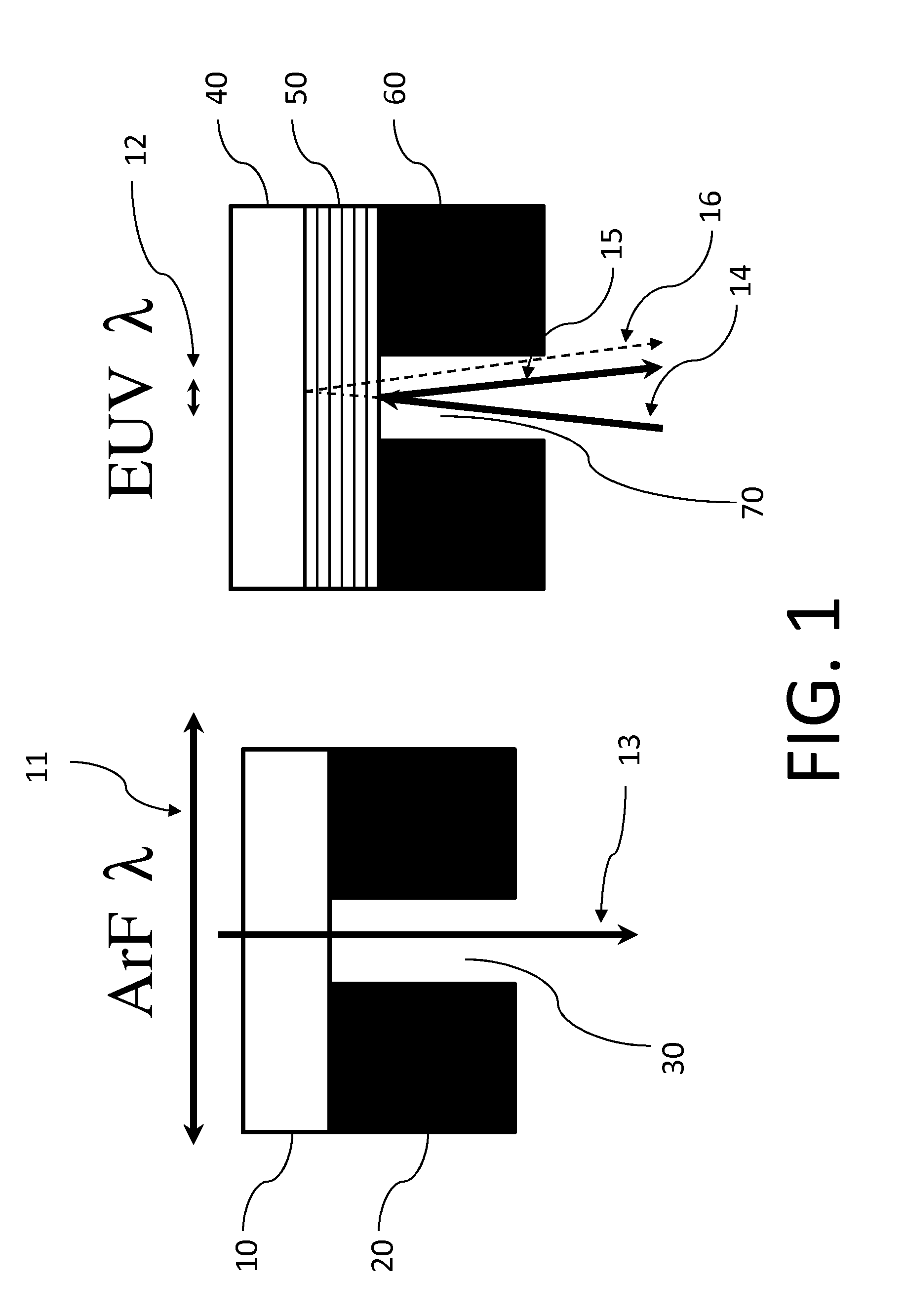
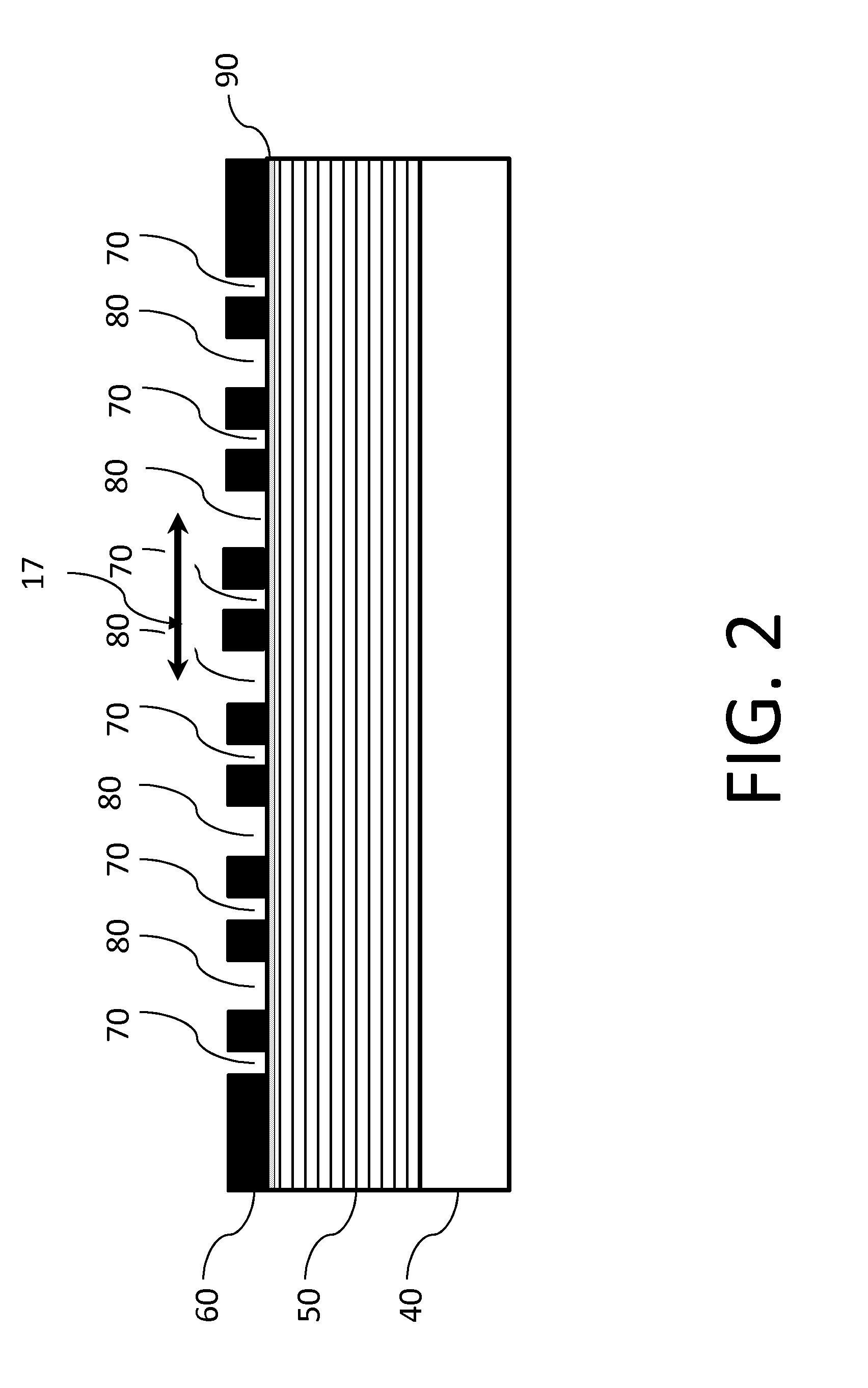
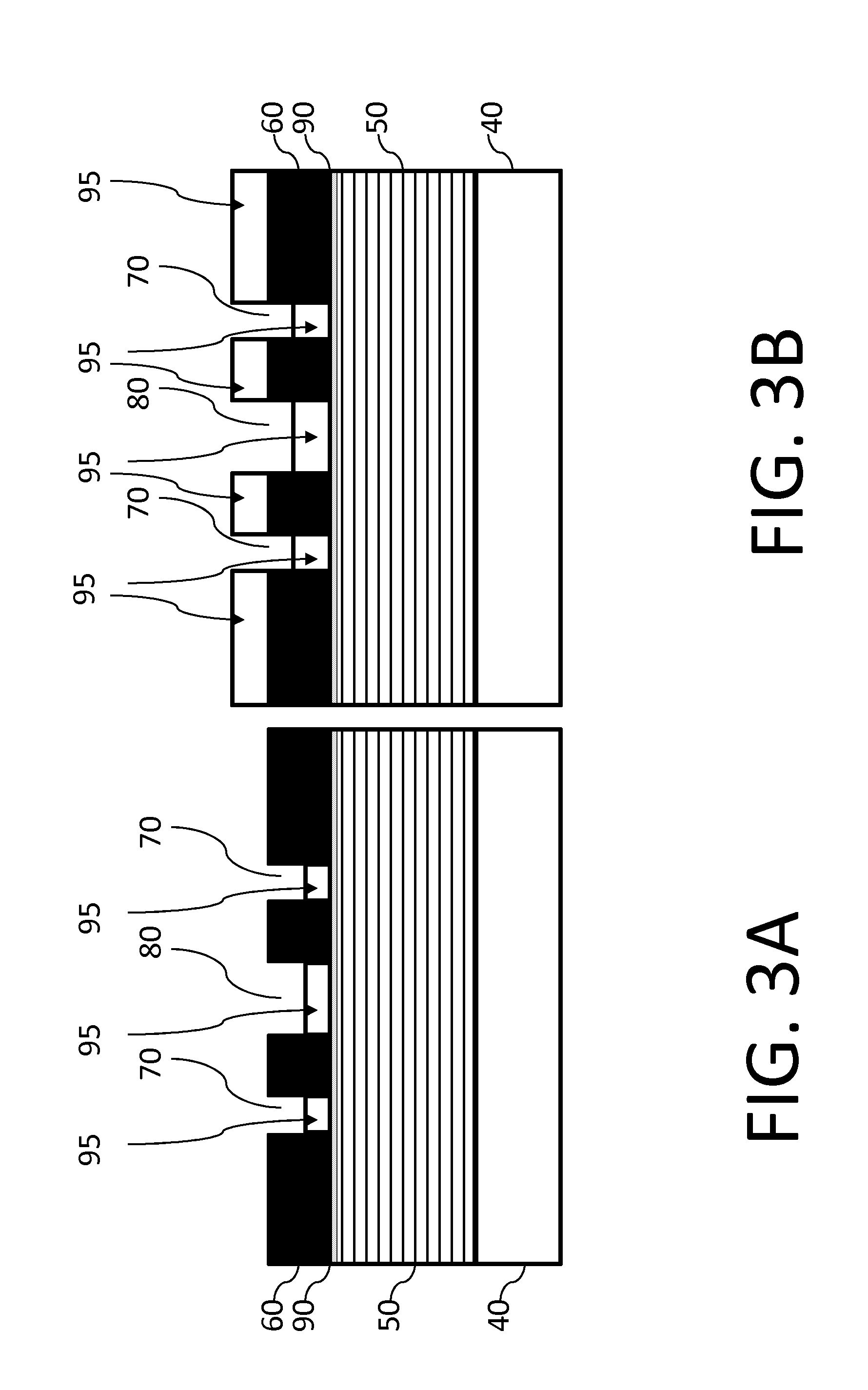
[0052]Referring to FIG. 6, this is a plot of trenchwidth versus focus for varying dose, or Bossung plot, on a wafer that was exposed with a 0.33 NA EUV scanner with a mask that had main features at 288 nm pitch in both cases, which are to be printed at 72 nm pitch on the wafer because the optics used a 4× demagnification. On the left side there are no assist features and the best focus is roughly in the center of the focus range at about −75 nm. Best focus is characterized as the point where there is negligible slope for the trenchwidth vs focus. On the right side, we plot the results from the same wafer with 72 nm pitch main features with assist features between them. The Bossung curve is sloped and there is no discernible best focus where the slope vanishes. This is due to the index mismatch between vacuum and absorber and this shift of best focus is what the invention is correcting.
example 2
[0053]FIG. 7A is a graphical representation of the quasar illumination that is typically used in high resolution lithography on the left, and FIG. 7B is a representation of the illumination that is used to investigate the various parts of this quasar illuminator in simulations whose results are shown in succeeding figures. The distance of an illuminator element from the center of illumination, represented as the center of the circle 100 in FIGS. 7A and 7B, is commonly denoted as σ (sigma), with σ=0 in the center and σ=1 at the edge of the circle. The representation of the quasar illuminator in FIG. 7A shows the angular distribution of the EUV light that is incident on the mask. The inner radius of the illumination in the experiments of FIG. 6 and simulations in FIGS. 8 through 10 is σ=0.37 and the outer radius is σ=0.88, which is a typical combination of inner and outer σ for printing a minimum pitch of 36 nm at a numerical aperture of 0.33 NA. If a different minimum pitch is requir...
example 3
[0054]FIG. 8 shows the trenchwidth vs. focus behavior for five different doses in simulation for various point quadrupoles as defined in FIG. 7B. The EUV system has a demagnification factor of 4. On the mask is a main opening of approximately 4 times the target size of the trench on the wafer, roughly 80 nm, at a pitch of 288 nm, and an assist feature size of 40 nm. The simulations are then performed to print 22 nm trenchwidth at a pitch of 72 nm. In the 7 sequential columns of FIG. 8, the distance of the poles 110 from the center of the illumination system defined by the circle 100 is sigma of 0.2 up to 0.8 in steps of 0.1. For the quadrupole at sigma=0.2, we have a trenchwidth vs. focus curve that has a strong down slope, or a strongly negative best focus position. For the settings of sigma=0.3 through 0.5, we have close to a centered best focus, while for sigma values of 0.6 and above the best focus has moved to very positive values. The final image in resist is a superposition o...
PUM
 Abstract
Description
Claims
Application Information