Group-III Nitride Epitaxial Layer on Silicon Substrate

a technology of nitride and silicon substrate, which is applied in the direction of semiconductor/solid-state device manufacturing, semiconductor devices, electrical devices, etc., can solve the problems of difficult to obtain gan bulk crystals, no readily available suitable substrate material, expensive and available,

Active Publication Date: 2009-10-22
TAIWAN SEMICON MFG CO LTD
View PDF5 Cites 47 Cited by
  • Summary
  • Abstract
  • Description
  • Claims
  • Application Information

AI Technical Summary

Benefits of technology

[0013]By using the embodiments of the present invention, group-III nitride layers can be formed over silicon (100) substrates, and hence making it possible to form optical devices on silicon (100) substrates.

Problems solved by technology

Due to the high equilibrium pressure of nitrogen at typical growth temperatures, it is extremely difficult to obtain GaN bulk crystals.
However, a current problem with the manufacture of GaN thin films is that there is no readily available suitable substrate material whose lattice constant and thermal expansion coefficient closely match that of GaN.
SiC is a semiconductor material providing excellent thermal conductivity, but is very expensive and available only in small wafer sizes.
Direct growth of GaN on SiC is generally difficult due to poor wetting between these materials.
In addition, it is very difficult to prepare a SiC layer having a smooth surface, while a rough interface with GaN can cause an increase in defect density of the GaN layer.
However, silicon (100) has a great lattice mismatch with GaN.
However, silicon (111) substrates are rarely used for conventional CMOS applications, and hence have relatively higher cost and less availability.

Method used


Image

  • Group-III Nitride Epitaxial Layer on Silicon Substrate
  • Group-III Nitride Epitaxial Layer on Silicon Substrate
  • Group-III Nitride Epitaxial Layer on Silicon Substrate

Examples


Embodiment Construction

[0017]The making and using of the presently preferred embodiments are discussed in detail below. It should be appreciated, however, that the present invention provides many applicable inventive concepts that can be embodied in a wide variety of specific contexts. The specific embodiments discussed are merely illustrative of specific ways to make and use the invention, and do not limit the scope of the invention.

[0018]A novel method for forming group-III nitride films and the resulting structures are provided. The intermediate stages of manufacturing preferred embodiments of the present invention are illustrated. The variations of the preferred embodiments are then discussed. Throughout the various views and illustrative embodiments of the present invention, like reference numbers are used to designate like elements.

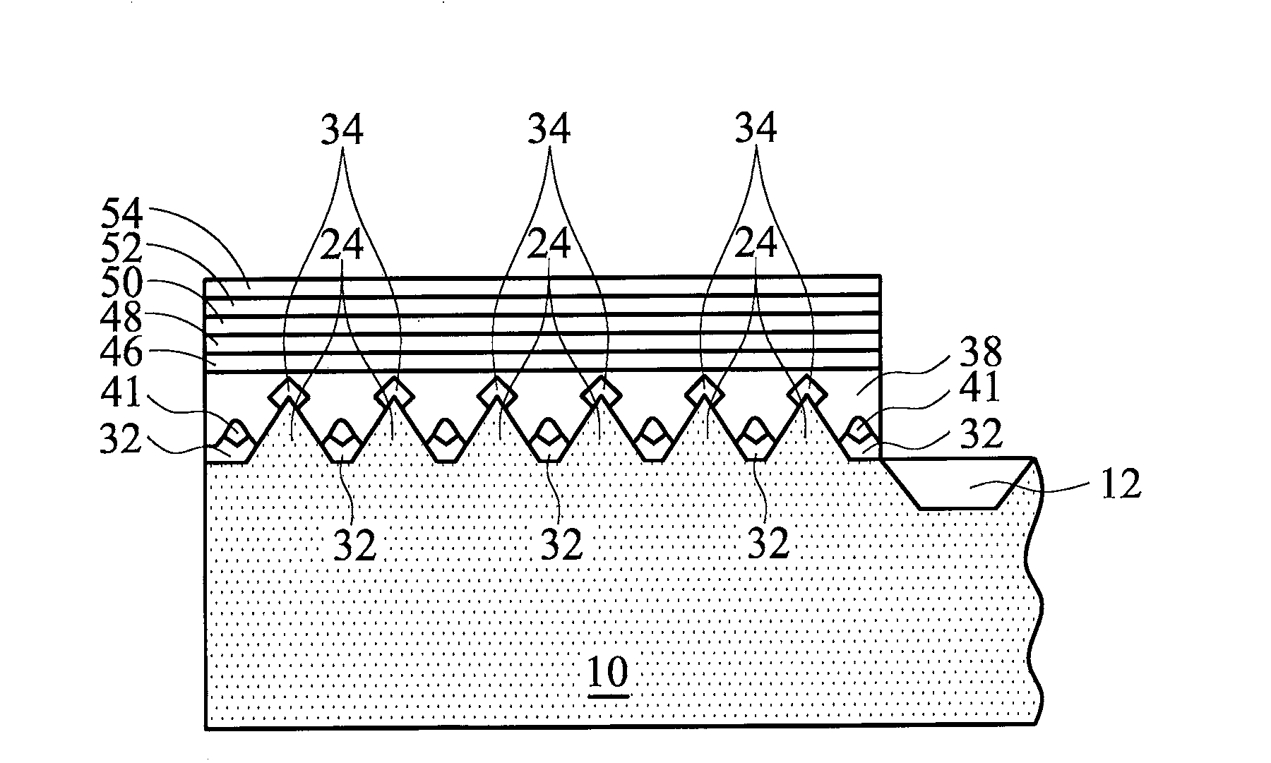
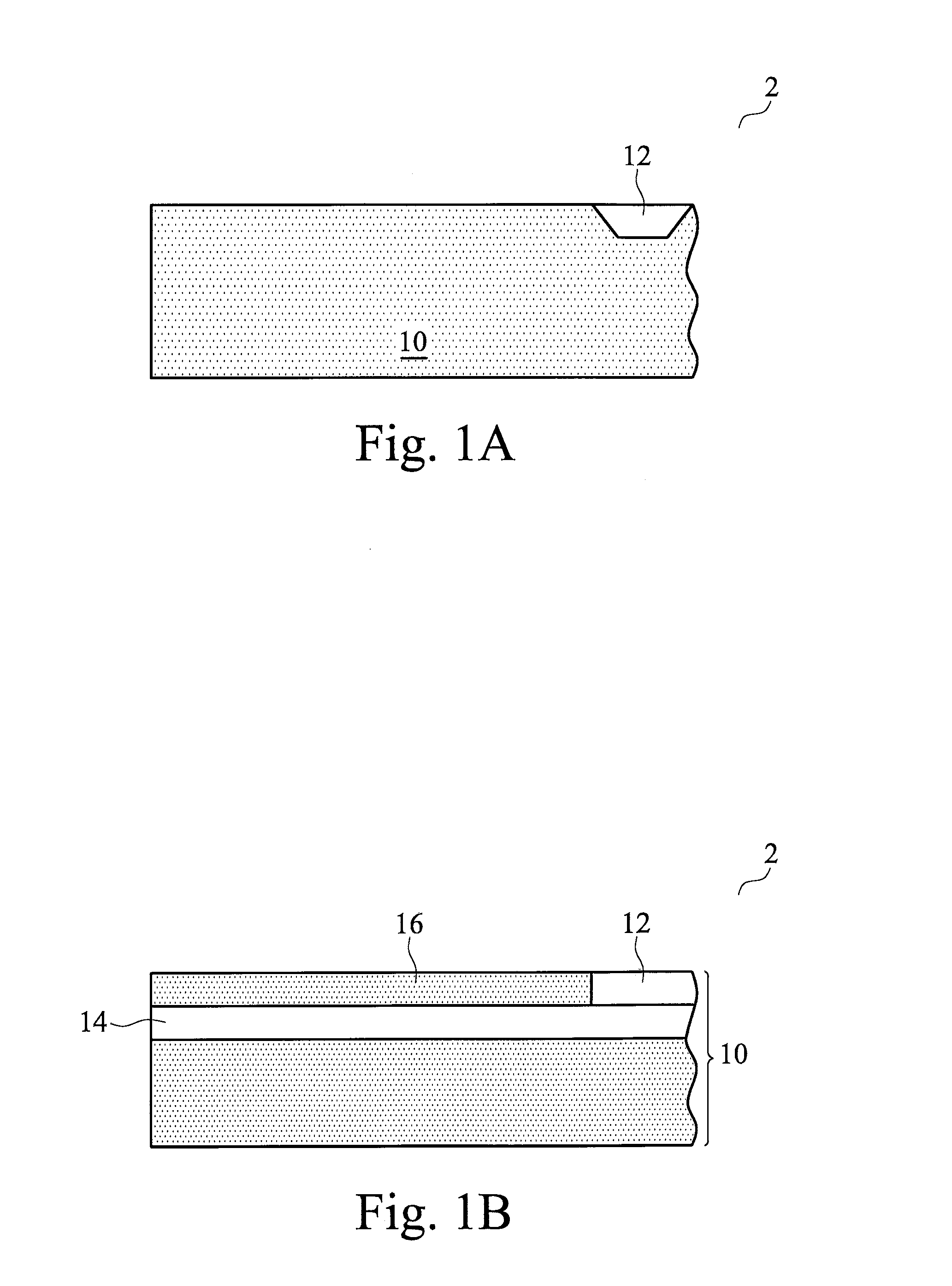
[0019]FIGS. 1A and 1B illustrate silicon substrate 10. In an embodiment, silicon substrate 10 is a (100) substrate having a (100) surface orientation, although it may hav...


PUM


Abstract

A semiconductor device includes a silicon substrate; silicon faceted structures formed on a top surface of the silicon substrate; and a group-III nitride layer over the silicon faceted structures. The silicon faceted structures are separated from each other, and have a repeated pattern.

Description

[0001]This application claims the benefit of the following provisionally filed U.S. Patent Application Ser. No. 61 / 045,504, filed Apr. 16, 2008, entitled “III-Nitride Epitaxial Layer on Patterned Silicon Substrate,” which application is hereby incorporated herein by reference.TECHNICAL FIELD[0002]This invention relates generally to semiconductor device manufacturing processes, and more particularly to forming crystalline group-III nitride films on silicon substrates.BACKGROUND[0003]Group-III nitride (often referred to as III-nitride or III-N) compounds, such as gallium nitride (GaN) and its related alloys, have been under intense research in recent years due to their promising applications in electronic and optoelectronic devices. Particular examples of potential optoelectronic devices include blue light emitting and laser diodes, and UV photo-detectors. The large bandgap and high electron saturation velocity of the III-nitride compounds also make them excellent candidates for appli...

Claims


Application Information

Patent Timeline
Patent Type & Authority Applications(United States)
IPC IPC(8): H01L33/00H01L33/12
CPCH01L21/02381H01L21/0243H01L21/02433H01L33/12H01L21/02639H01L33/007H01L21/0254
Inventor CHEN, DING-YUANYU, CHEN-HUA
Owner TAIWAN SEMICON MFG CO LTD
Why Eureka
Try Eureka