
Organic light emitting display

a light-emitting display and organic technology, applied in static indicating devices, electroluminescent light sources, instruments, etc., can solve problems such as scratching of flattening films, and achieve the effect of preventing shortening

Active Publication Date: 2008-03-06
SAMSUNG DISPLAY CO LTD
View PDF5 Cites 9 Cited by
  • Summary
  • Abstract
  • Description
  • Claims
  • Application Information

AI Technical Summary

Benefits of technology

[0032]The present invention provides an organic light emitting display capable of preventing wires disposed on a non-display region from being shorted.
[0056]In the organic light emitting display having the aforementioned structure, the signal lines are prevented from being shorted. Accordingly, serious errors are prevented from occurring in driving the organic light emitting devices.

Problems solved by technology

However, when the part of the encapsulation glass is removed, the flattening film is scratched by glass particles generated in the scribing process.

Method used


Image

  • Organic light emitting display
  • Organic light emitting display
  • Organic light emitting display

Examples


Embodiment Construction

[0062]The present invention will now be described more fully hereinafter with reference to the accompanying drawings, in which preferred embodiments of the invention are shown. As those skilled in the art would realize, the described embodiments may be modified in various different ways, all without departing from the spirit or scope of the present invention.

[0063]Like reference numerals designate like elements throughout the specification.

[0064]In the drawings, the thickness of layers, films, panels, regions, etc. are exaggerated for clarity. It will be understood that when an element such as a layer, film, region or substrate is referred to as being “on” another element, it can be directly on the other element or intervening elements may also be present.

[0065]In contrast, when an element is referred to as being “directly on” another element, there are no intervening elements present.

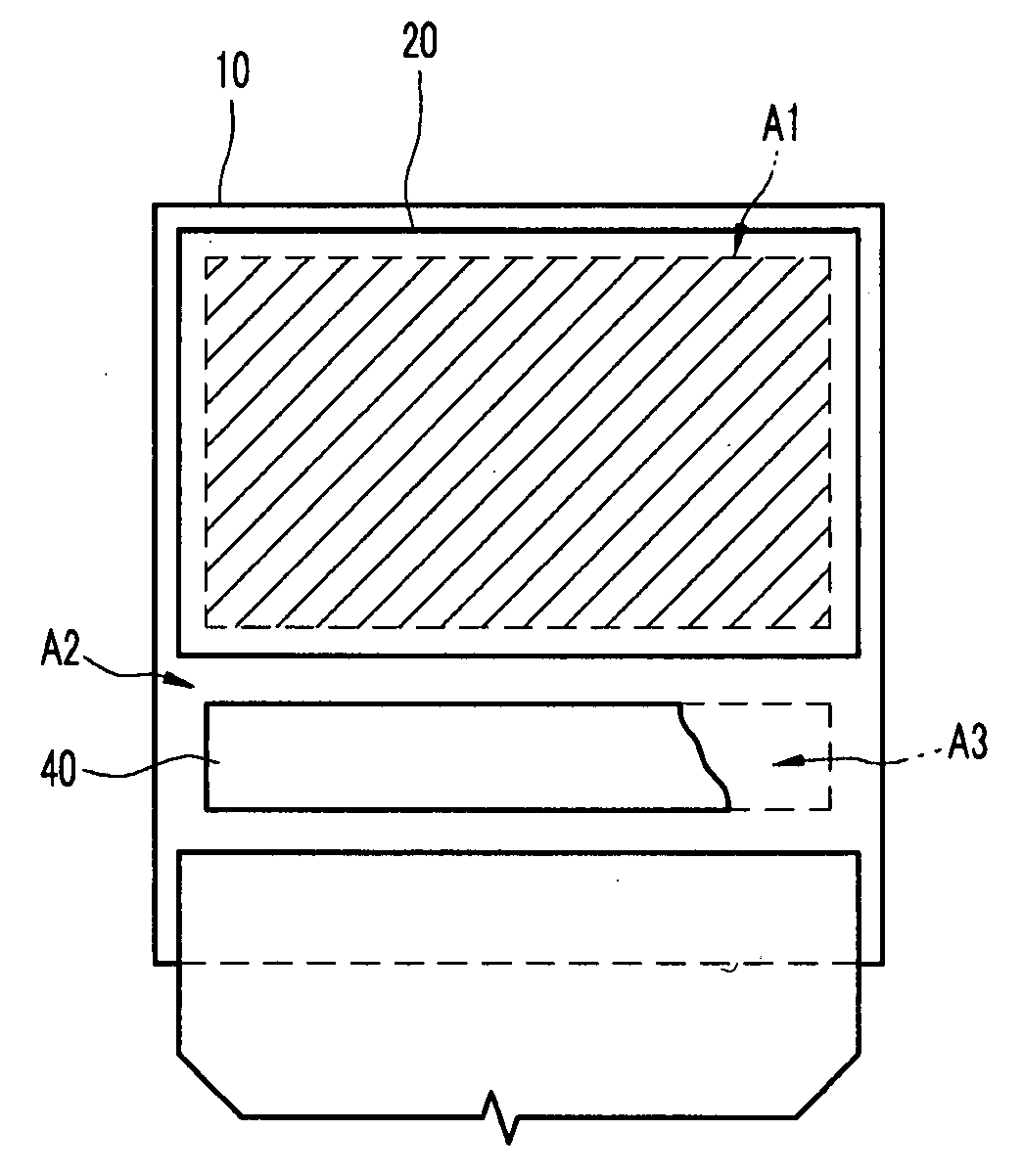
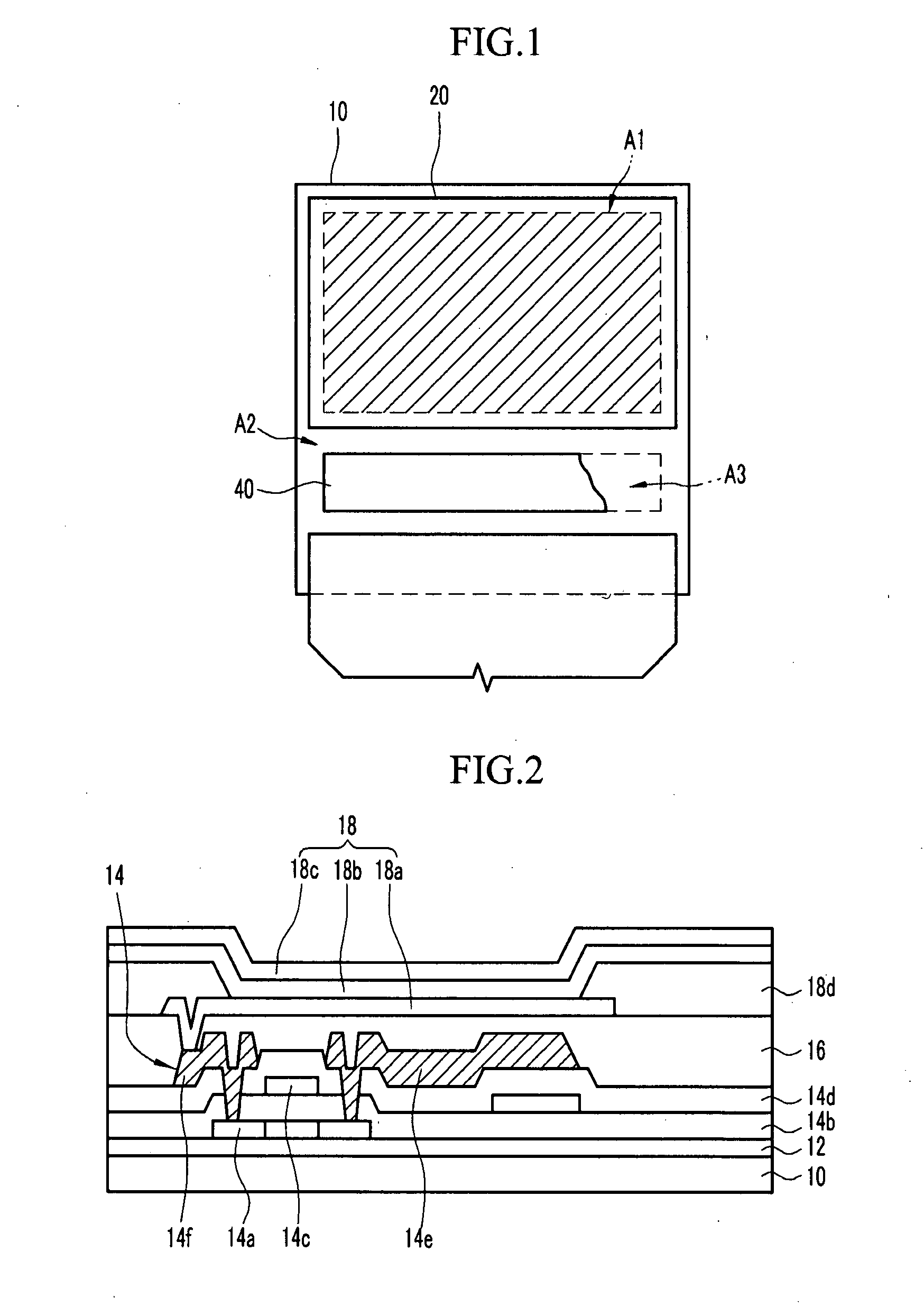
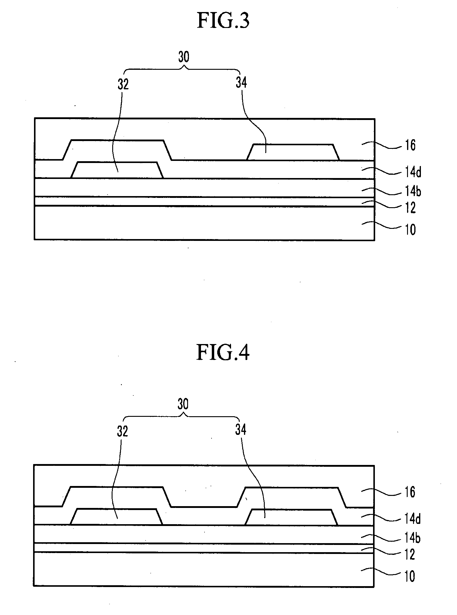
[0066]FIG. 1 is a top plan view illustrating a schematic structure of an organic light emitting dis...


PUM


Abstract

An organic light emitting display is provided. In the organic light emitting display, when a wiring section including a plurality of signal lines for transmitting signals to a driving circuit unit or an organic light emitting device is formed under a non-display region, more specifically, a COG region where a driving IC is mounted, the signal lines of the wiring section are disposed on two or more different layers to maintain a height difference between neighboring signal lines for transmitting different signals from each other.

Description

CROSS-REFERENCE TO RELATED APPLICATION[0001]This application claims priority to and the benefit of Korean Patent Application No. 10-2006-0083527 filed in the Korean Intellectual Property Office on Aug. 31, 2006, the entire content of which is incorporated herein by reference.BACKGROUND OF THE INVENTION[0002]1. Field[0003]The present invention relates to an organic light emitting display, and more particularly, to an organic light emitting display in which signal lines disposed under a non-display region located out of a display region where an image is displayed, more specifically, a chip on glass (COG) region are prevented from being shorted.[0004]2. Description of the Related Art[0005]Recently, various flat displays capable of reducing weight and volume compare to cathode ray tube (CRT) displays are being developed.[0006]The flat display devices include a liquid crystal display (LCD), a field emission display (FED), a plasma display panel (PDP), an organic light emitting display (...

Claims


Application Information

Patent Timeline
IPC IPC(8): G09G3/32
CPCH01L51/5237H01L27/3276H10K59/131H10K59/871H05B33/26H10K50/841
Inventor KIM, EUN-AH
Owner SAMSUNG DISPLAY CO LTD
Learn More