

Solid-state imaging device
- Summary
- Abstract
- Description
- Claims
- Application Information
AI Technical Summary
Benefits of technology
Problems solved by technology
Method used
Image

Examples
first embodiment
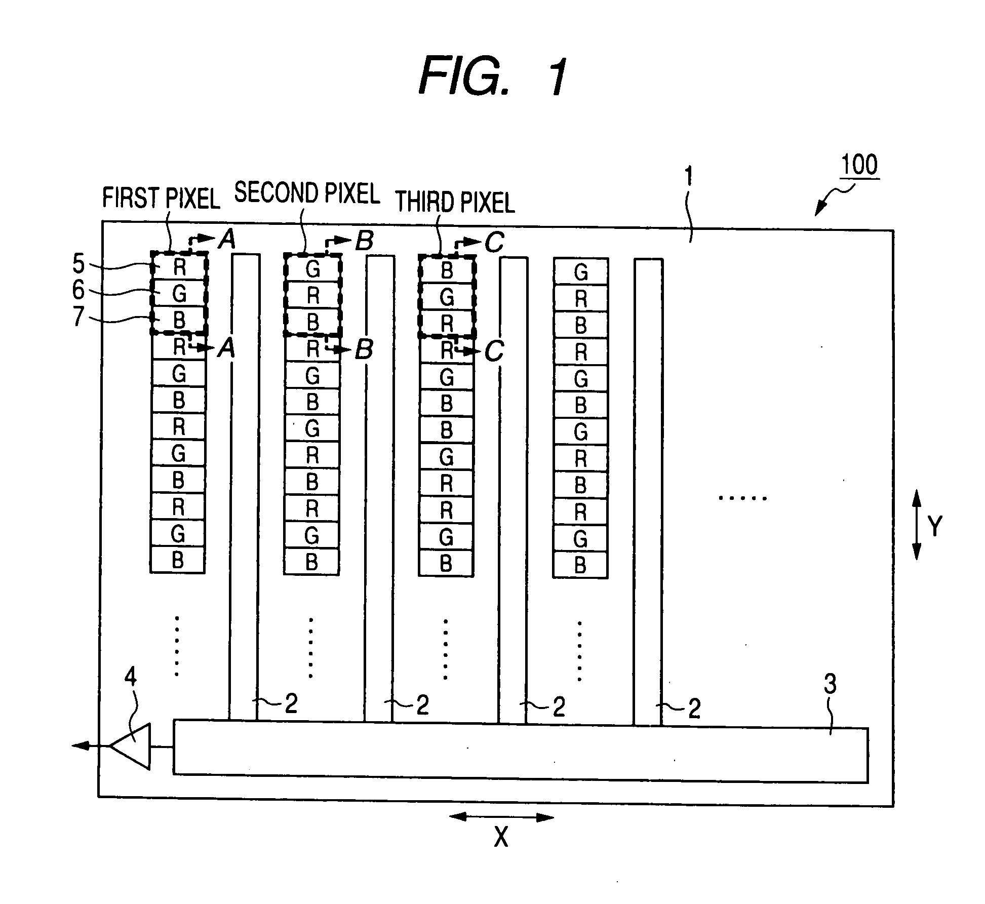
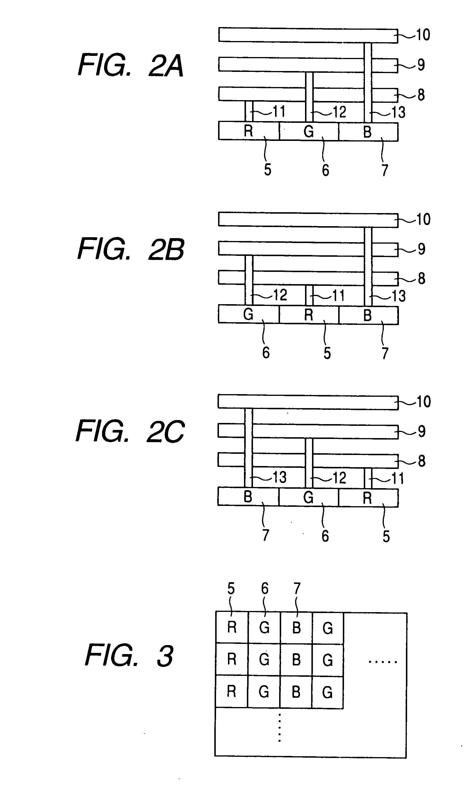
[0046]FIG. 1 is a diagrammatic plan view of a solid-state imaging device for describing a first exemplary embodiment of the invention. FIG. 2A is a diagrammatic sectional view of the solid-state imaging device taken along the line A-A shown in FIG. 1. FIG. 2B is a diagrammatic sectional view of the solid-state imaging device taken along the line B-B shown in FIG. 1. FIG. 2C is a diagrammatic sectional view of the solid-state imaging device taken along the line C-C shown in FIG. 1.
[0047]As shown in FIGS. 2A to 2C (sometimes referred to as “FIG. 2”), a solid-state imaging device 100 has a red (R) light photoelectric conversion layer 8 for detecting red light and generating corresponding red-light signal charges, a green (G) light photoelectric conversion layer 9 for detecting green light and generating corresponding green-light signal charges, and a blue (B) photoelectric conversion layer 10 for detecting blue light and generating corresponding blue-light signal charges. Those films a...
second embodiment
[0062]In a solid-state imaging device 300 for describing this embodiment, the signal charge accumulators 5 to 7 are reconfigured such that each of the first to third arrays of the solid-state imaging device 200 shown in FIG. 4 has a longitudinal stripe layout in which all of the signal charge accumulators 5 to 7 are included.
[0063]FIG. 5 is a diagrammatical plan view of a solid-state imaging device for describing the second embodiment of the invention. FIG. 6A is a diagrammatic sectional view of the solid-state imaging device taken along the line A-A shown in FIG. 5. FIG. 6B is a diagrammatic sectional view of the solid-state imaging device taken along the line B-B shown in FIG. 5. FIG. 6C is a diagrammatic sectional view of the solid-state imaging device taken along the line C-C shown in FIG. 5. In FIGS. 5 and 6A to 6C, similar structures to those in FIGS. 2 and 4 have the same characters.
[0064]Among a large number of pixels of the solid-state imaging device 300, there are included...
third embodiment
[0071]In a solid-state imaging device 400 for describing this embodiment, the signal charge accumulators 5 to 7 are reconfigured such that the first array of the solid-state imaging device 200 shown in FIG. 4 has a lateral stripe layout in which all of the signal charge accumulators 5 to 7 are included.
[0072]FIG. 9 is a diagrammatical plan view of a solid-state imaging device for describing the third embodiment of the invention. FIG. 10 is a diagrammatic sectional view of the solid-state imaging device taken along the line A-A shown in FIG. 9. In FIGS. 9 and 10, similar structures to those in FIGS. 2 and 4 have the same characters.
[0073]Among a large number of pixels of the solid-state imaging device 400, there are included the first pixel having the signal charge accumulator 5, the signal charge accumulator 6, and the signal charge accumulator 7 arranged columnwise in this order, the fourth pixel having the signal charge accumulator 6, the signal charge accumulator 7, and the signa...
PUM
 Abstract
Description
Claims
Application Information