Flash memory device including unified oscillation circuit and method of operating the device

a flash memory and oscillation circuit technology, applied in static storage, digital storage, instruments, etc., can solve the problems of unexpected change or glitch of internal clock signal cycle, and achieve the effect of reducing the incidence of timing glitches and improving circuit density

Active Publication Date: 2008-03-06
SAMSUNG ELECTRONICS CO LTD
View PDF4 Cites 3 Cited by
  • Summary
  • Abstract
  • Description
  • Claims
  • Application Information

AI Technical Summary

Benefits of technology

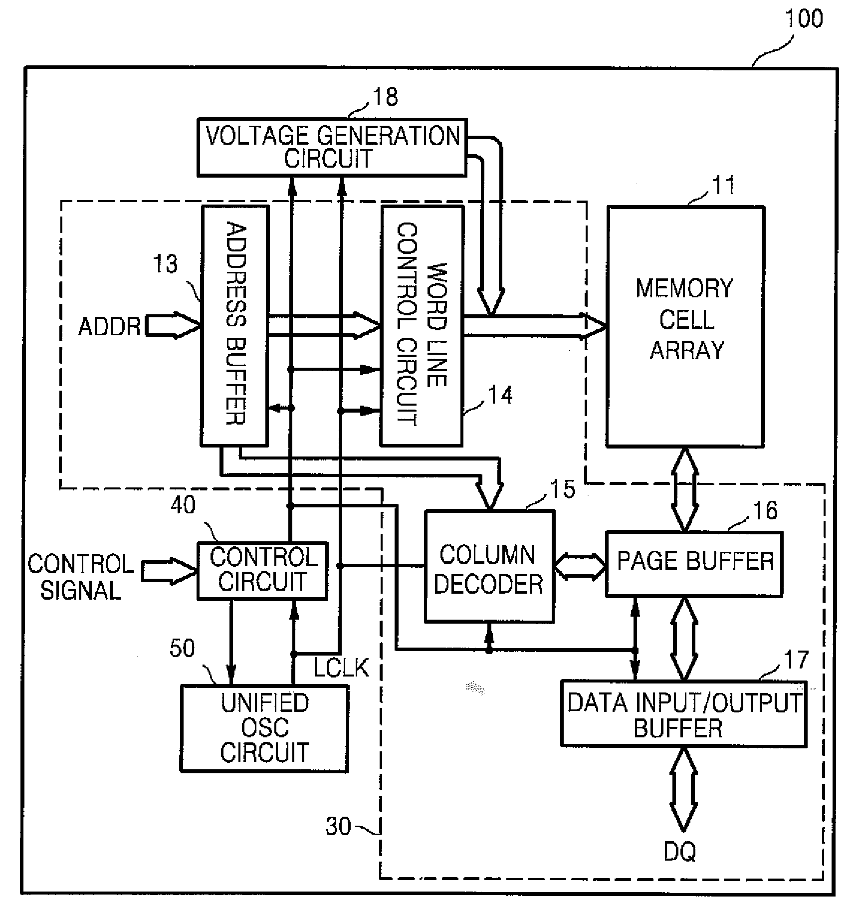
[0014]Embodiments of the present invention provide a flash memory device with a unified oscillation circuit, and a method of operating the device. The unified oscillation circuit produces alternative internal clock signals for corresponding alternative operating modes of the flash memory device. At least a portion of the unified oscillation circuit is used to generate all of the alternative internal clock signals. Compared to conventional memory devices and methods that use multiple oscillators, embodiments of the invention improve circuit density and reduce the incidence of timing glitches caused by switching between multiple oscillators.

Problems solved by technology

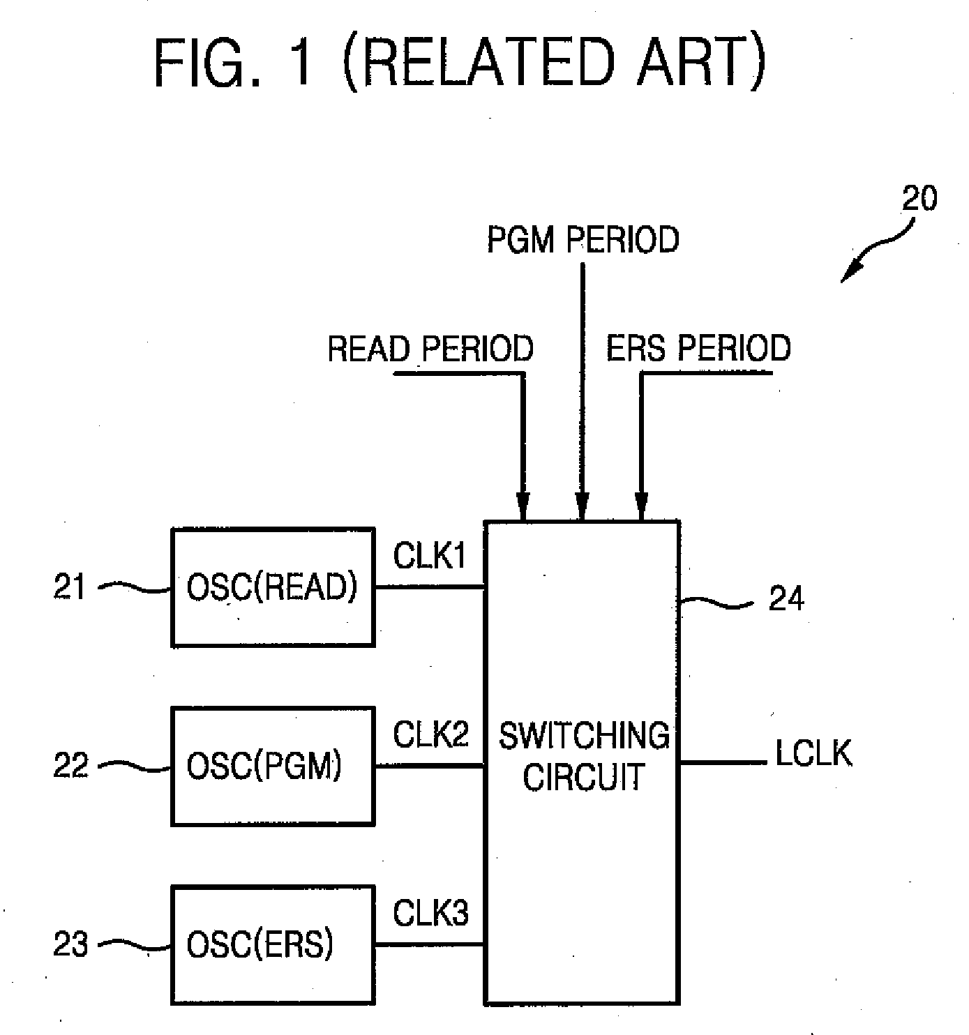
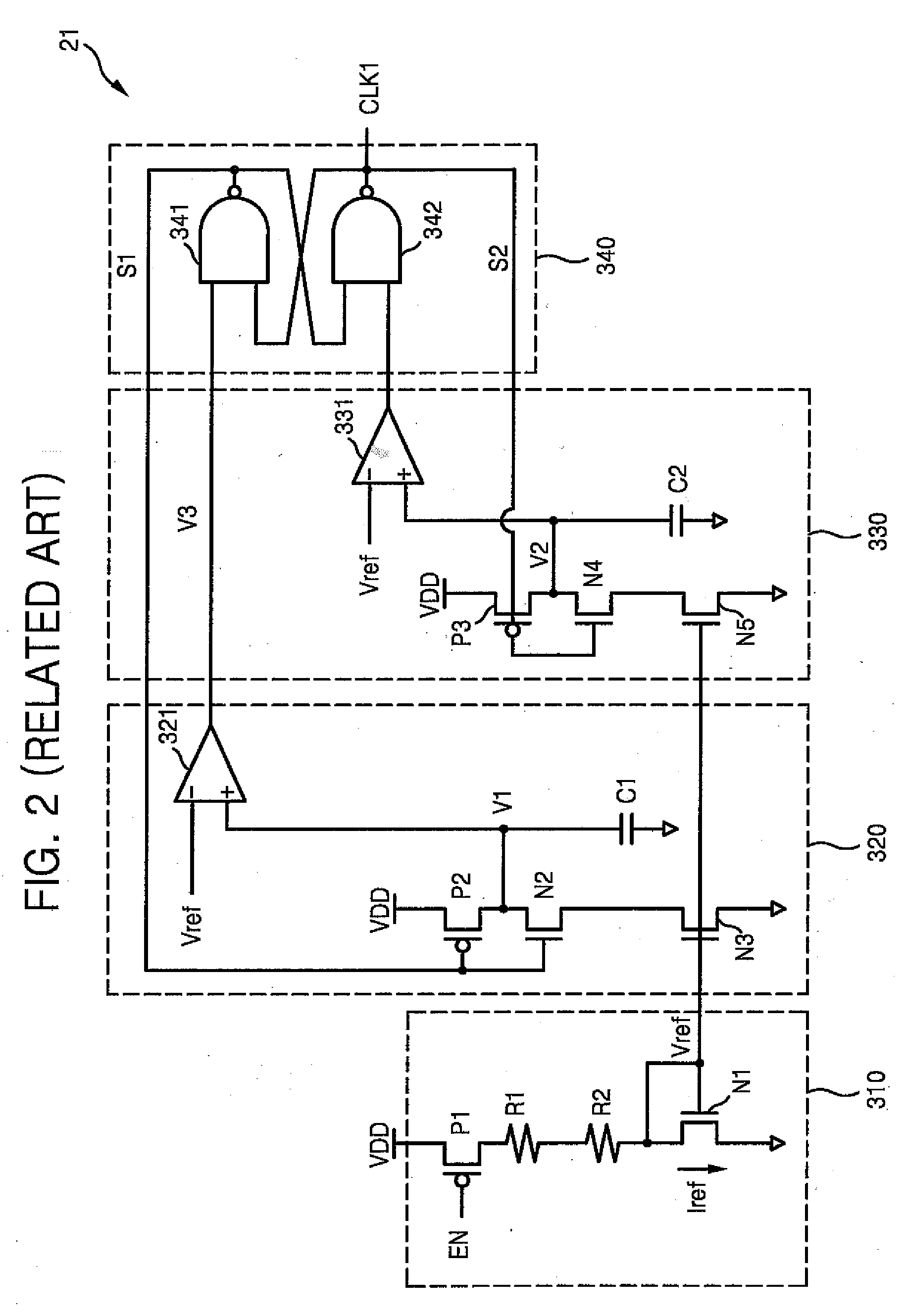
Although it is possible to adjust the cycle according to an operating mode, oscillators need to be switched when the operating mode is changed At the moment of switching of two oscillators, the cycle of the internal clock signal may unexpectedly change or a glitch may occur.

Method used


Image

  • Flash memory device including unified oscillation circuit and method of operating the device
  • Flash memory device including unified oscillation circuit and method of operating the device
  • Flash memory device including unified oscillation circuit and method of operating the device

Examples


Embodiment Construction

[0026]The present invention now will be described more fully hereinafter with reference to the accompanying drawings, in which embodiments of the invention are shown. This invention may, however, be embodied in many different forms and should not be construed as limited to the embodiments set forth herein. Rather, these embodiments are provided so that this disclosure will be thorough and complete, and will fully convey the scope of the invention to those skilled in the art. In the drawings, like numbers refer to like elements throughout.

[0027]It will be understood that when an element is referred to as being “connected” or “coupled” to another element, it can be directly connected or coupled to the other element or intervening elements may be present. In contrast, when an element is referred to as being “directly connected” or “directly coupled” to another element, there are no intervening elements present. As used herein, the term “and / or” includes any and all combinations of one ...


PUM


Abstract

Embodiments of the present invention provide a flash memory device with a unified oscillation circuit, and a method of operating the device. The unified oscillation circuit produces alternative internal clock signals for corresponding alternative operating modes of the flash memory device. At least a portion of the unified oscillation circuit is used to generate all of the alternative internal clock signals. Compared to conventional memory devices and methods that use multiple oscillators, embodiments of the invention improve circuit density and reduce the incidence of timing glitches caused by switching between multiple oscillators.

Description

BACKGROUND OF THE INVENTION[0001]1. Field of the Invention[0002]The present invention relates to a semiconductor memory device, and more particularly, to a flash memory device.[0003]This application claims the benefit of Korean Patent Application No. 10-2006-0085454, filed on Sep. 6, 2006, in the Korean Intellectual Property Office, the disclosure of which is incorporated herein in its entirety by reference.[0004]2. Description of Related Art[0005]Generally, flash memory devices have three main operating modes, i.e., a program mode, an erase mode, and a read mode. The cycle of an internal clock signal, which is required in an internal circuit of a flash memory device, is different according to an operating mode. Conventional flash memory devices include separate oscillation circuits for the respective operating modes in order to generate internal clock signals having different cycles according to the operating modes.[0006]Meanwhile, flash memory devices need high voltage to erase an...

Claims


Application Information

Patent Timeline
Patent Type & Authority Applications(United States)
IPC IPC(8): G11C16/04G11C16/06
CPCG11C16/32G11C16/0483G11C16/10G11C16/26
Inventor KIM, JIN-KOOKLEE, JIN-YUB
Owner SAMSUNG ELECTRONICS CO LTD
Why Eureka
Try Eureka