Structure and manufacturing process for circuit board

Active Publication Date: 2009-11-19
UNIMICRON TECH CORP
View PDF8 Cites 6 Cited by
  • Summary
  • Abstract
  • Description
  • Claims
  • Application Information

AI Technical Summary

Benefits of technology

[0021]Accordingly, while the fine circuit pattern is inlaid in the dielectric layer or the composite layer, since a conductive circuit having a fine line width and spacing can be fabricated, wiring density of the circuit board structure can be increased.

Problems solved by technology

However, due to limitation of the conventional fabrication process for the circuit board, i.e. limitation of line width and spacing of a fine circuit, a wiring density of the circuit board fabricated based on the aforementioned method cannot be increased.

Method used


Image

  • Structure and manufacturing process for circuit board
  • Structure and manufacturing process for circuit board
  • Structure and manufacturing process for circuit board

Examples


first embodiment

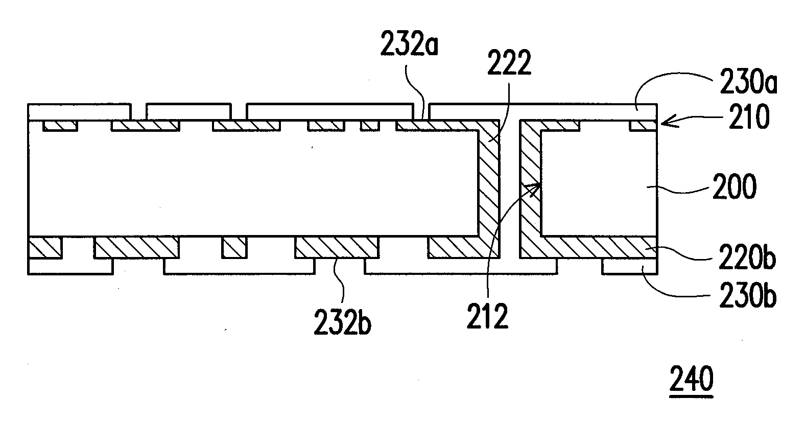
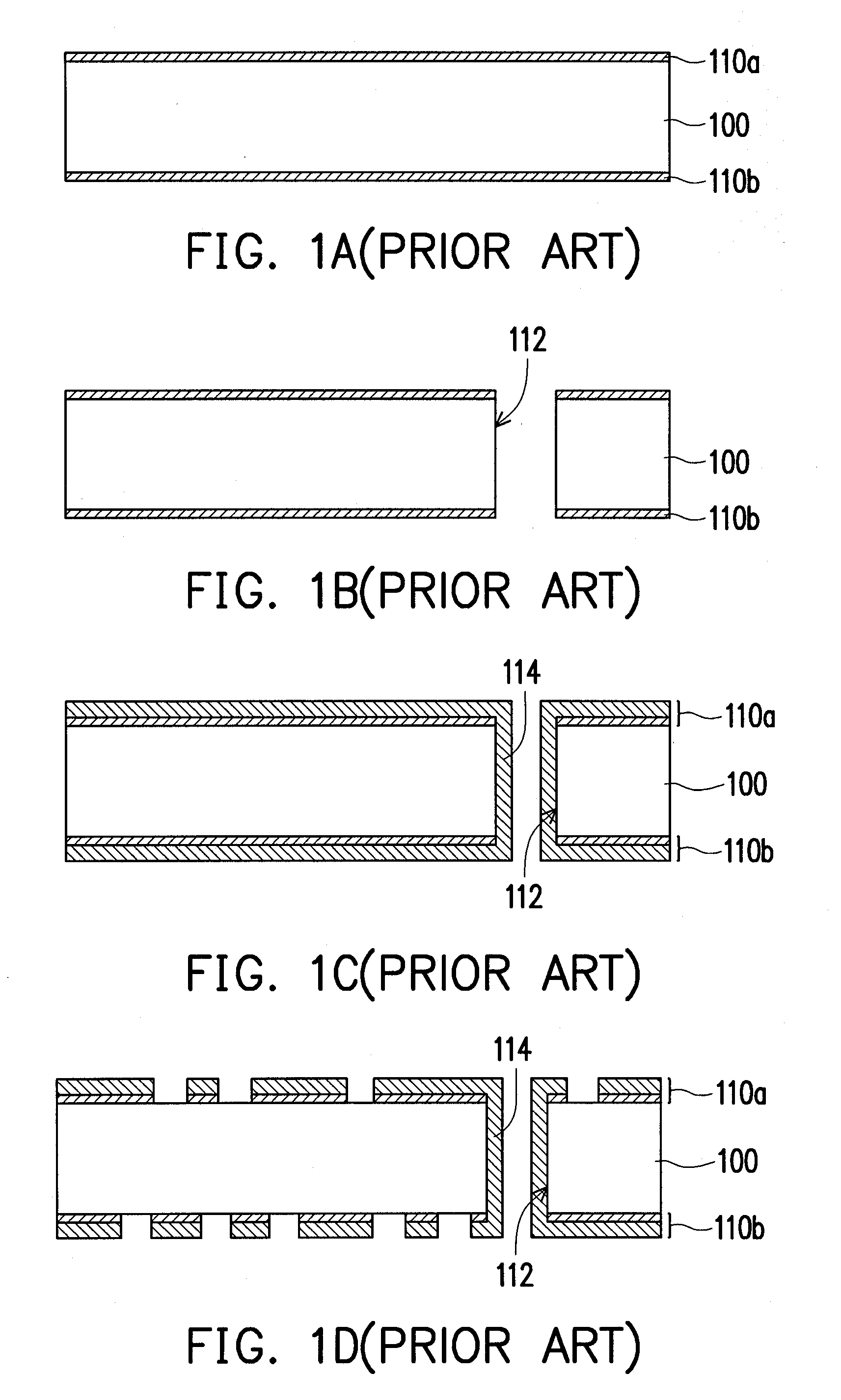
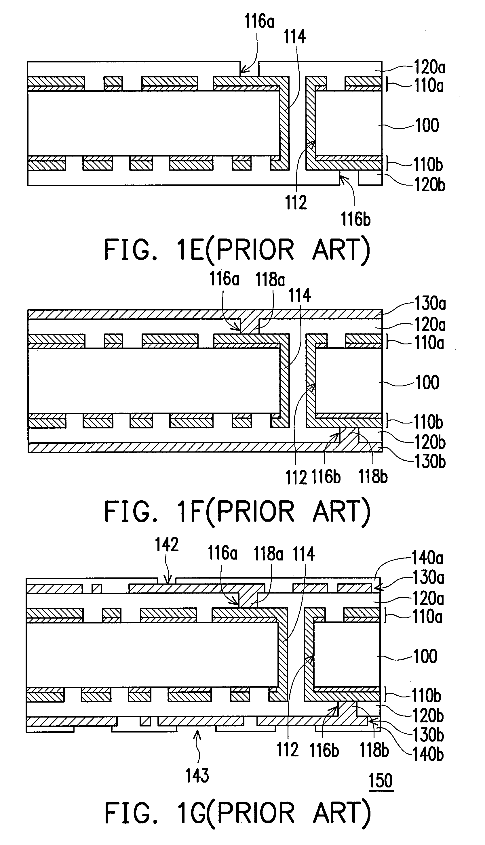
[0028]In the first embodiment of the present invention, fabrication process of a circuit board with double conductive layers is described. FIGS. 2A-2F are profile flowcharts illustrating a fabrication process for a circuit board according to a first embodiment of the present invention.

[0029]Referring to FIG. 2A, a plate utilized in the beginning of the fabrication process can be a dielectric layer 200, and the material thereof can be epoxy resin or epoxy resin containing glass fiber.

[0030]Referring to FIG. 2B, fine circuit grooves 200a are formed on a surface of the dielectric layer 200 by for example, laser ablating, and at least one through hole 212 is formed in the dielectric layer 200 by mechanical drilling or the laser ablating.

[0031]Referring to FIG. 2C, the conductive material (for example, copper) is filled in the fine circuit grooves 200a by for example, electroplating, so as to form a fine circuit pattern 210 inlaid in the surface of the dielectric layer 200. Moreover, whi...

second embodiment

[0036]In the second embodiment of the present invention, fabrication process of a circuit board with double conductive layers is described. FIGS. 3A-3F are profile flowcharts illustrating a fabrication process for a circuit board according to a second embodiment of the present invention.

[0037]Referring to FIG. 3A, a plate utilized in the beginning of the fabrication process can be a dielectric layer 300, and the material thereof can be epoxy resin or epoxy resin containing glass fiber.

[0038]Referring to FIG. 3B, fine circuit grooves 300a are formed on a surface of the dielectric layer 300 by for example, laser ablating, and at least one through hole 312 is formed in the dielectric layer 300 by mechanical drilling or the laser ablating.

[0039]Referring to FIG. 3C, the conductive material (for example, copper) is filled in the fine circuit grooves 300a by for example, electroplating, so as to form a fine circuit pattern 310 inlaid in the surface of the dielectric layer 300. Moreover, w...

third embodiment

[0044]In the third embodiment of the present invention, fabrication process of a circuit board with multiple conductive layers (in the present embodiment, four conductive layers are applied) is described. FIGS. 4A-4F are profile flowcharts illustrating a fabrication process for a circuit board according to a third embodiment of the present invention.

[0045]Referring to FIG. 4A, a plate utilized in the beginning of the fabrication process can be a composite layer 400 including three dielectric layers 401, 402 and 403, two patterned conductive layers 404 and 405, and at least one conductive via 406. Material of the dielectric layers 401, 402 and 403 can be epoxy resin or epoxy resin containing glass fiber, etc., and material of the patterned conductive layers 404 and 405 can be coppers, etc. The conductive via 406 electrically connects the patterned conductive layers 404 and 405, and has a shape of a hollow cylinder shown in FIG. 4A or a solid cylinder which is not shown. Since fabrica...


PUM

PropertyMeasurementUnit
Dielectric polarization enthalpyaaaaaaaaaa
Shapeaaaaaaaaaa
Electrical conductoraaaaaaaaaa

Abstract

A circuit board structure comprising a composite layer, a fine circuit pattern and a patterned conductive layer is provided. The fine circuit pattern is inlaid in the composite layer, and the patterned conductive layer is disposed on a surface of the composite layer. After fine circuit grooves are formed on the surface of the composite layer, conductive material is filled into the grooves to form the fine circuit pattern inlaid in the composite layer. Since this fine circuit pattern has relatively fine line width and spacing, the circuit board structure has a higher wiring density.

Description

CROSS-REFERENCE TO RELATED APPLICATION[0001]This application claims the priority benefit of Taiwan application serial no. 97117556, filed on May 13, 2008. The entirety of the above-mentioned patent application is hereby incorporated by reference herein and made a part of specification.BACKGROUND OF THE INVENTION[0002]1. Field of the Invention[0003]The present invention relates to a circuit structure and a manufacturing process for a circuit board. More particularly, the present invention relates to a circuit structure and manufacturing process for a circuit board having higher wiring density.[0004]2. Description of Related Art[0005]A conventional circuit board is mainly formed by alternately stacking a plurality of patterned conductive layers and a plurality of dielectric layers, wherein the patterned conductive layers are electrically connected through a plurality of conductive vias. Discriminated based on fabrication processes of the circuit boards, the fabrication processes mainl...

Claims


Application Information

Patent Timeline
IPC IPC(8): H05K3/10H05K1/00
CPCH05K1/0265H05K3/045H05K3/107H05K3/426H05K3/465H05K2201/0352Y10T29/49126H05K1/02H05K1/0298H05K1/115Y10T29/49117Y10T29/49155Y10T29/4913H05K2201/09736
Inventor CHEN, TSUNG-YUANCHIANG, SHU-SHENGCHENG, DAVID C. H.
Owner UNIMICRON TECH CORP
Why Eureka
Try Eureka