Method For Fabricating Integrated Circuit Features

a technology of integrated circuits and features, applied in the field of integrated circuit fabrication, can solve the problems of inability of optical lithography to fabricate ic features with the prior art method of optical lithography is problematic, and the inability of optical lithography to achieve such diminutive line widths, so as to prevent the expansion of edge based image transfer shapes, save costs, and optimize use

Inactive Publication Date: 2007-05-10
GOOGLE LLC
View PDF15 Cites 2 Cited by
  • Summary
  • Abstract
  • Description
  • Claims
  • Application Information

AI Technical Summary

Benefits of technology

[0014] According to a fourth embodiment of the invention, a set of edge based image transfer shapes is selected in the plurality for the optimized number of edge based image transfer shapes in the IC pattern and exclusion areas are defined around the set, substantially preventing expansion of edge based image transfer shapes that would cause at least partial IC failure in response to edge based image expansion.
[0015] The present invention optimizes use of edge based image transfer in cooperation with optical lithography for fabrication of an integrated circuit. In so doing, the present invention saves costs because dual features are created with edge based image transfer, improves upon circuit density because edge based image transfer process are created with tight dimensional control, and yet compensates for any deficiencies of the edge based image transfer process through continued reliance on optical lithography.

Problems solved by technology

The prior art method of optical lithography is problematic because optical lithography tools are limited by the light source's wavelength.
As IC features shrink to, for example, line widths of 45.0 nm, the inability of optical lithography to fabricate IC features with such diminutive line widths becomes increasingly problematic.
Diffraction effects, however, limit optical lithography's ability to deliver such dimensionally controlled IC features.
The IC features produced by optical lithography are limited to line widths greater than the minimum resolution of the optical lithography tool, which is ultimately limited by the wavelength (“λ”) of the light source used by the optical lithography tool to expose the resist.
For at least these reasons, optical lithography is deficient.
While SIT has improved dimensional control over the prior art method of optical lithography, the prior art method SIT is problematic because only one IC feature size can be fabricated per SIT operation, only closed loop topographies can be created, and SIT has an incomprehensive IC feature shape library, in other words, only certain IC feature shapes can be fabricated with SIT.
While dimensional control is important, sometime dimensional control is secondary to other considerations, e.g. larger feature size, chip performance, and cost.
In addition to these considerations, SIT is disadvantageous because only a limited number of shapes, and more specifically closed loop shapes, can be created by SIT.
Another reason that SIT is problematic is the challenge associated with the translation of the IC layout to the mask set required to exercise edge based imaging process.
In sum, while SIT improves upon dimensional control, SIT does not entirely eliminate reliance on optical lithography.

Method used


Image

  • Method For Fabricating Integrated Circuit Features
  • Method For Fabricating Integrated Circuit Features
  • Method For Fabricating Integrated Circuit Features

Examples


Embodiment Construction

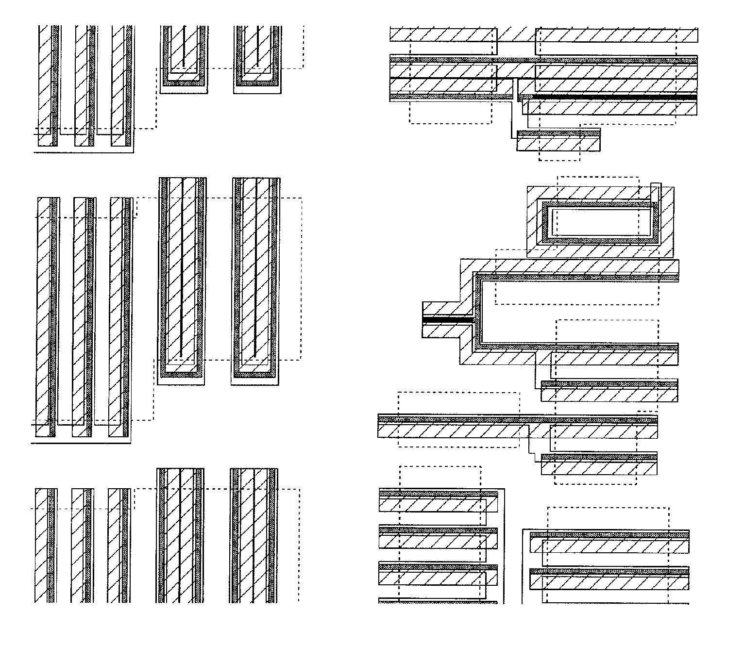
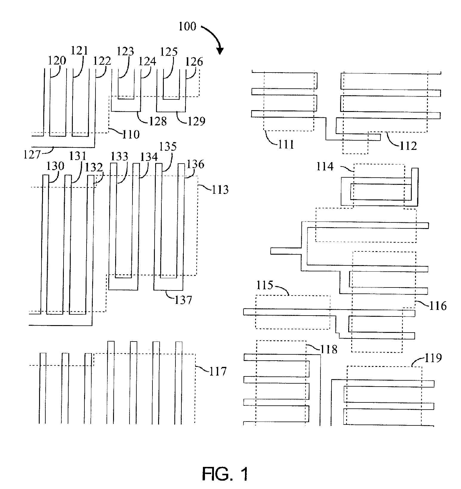
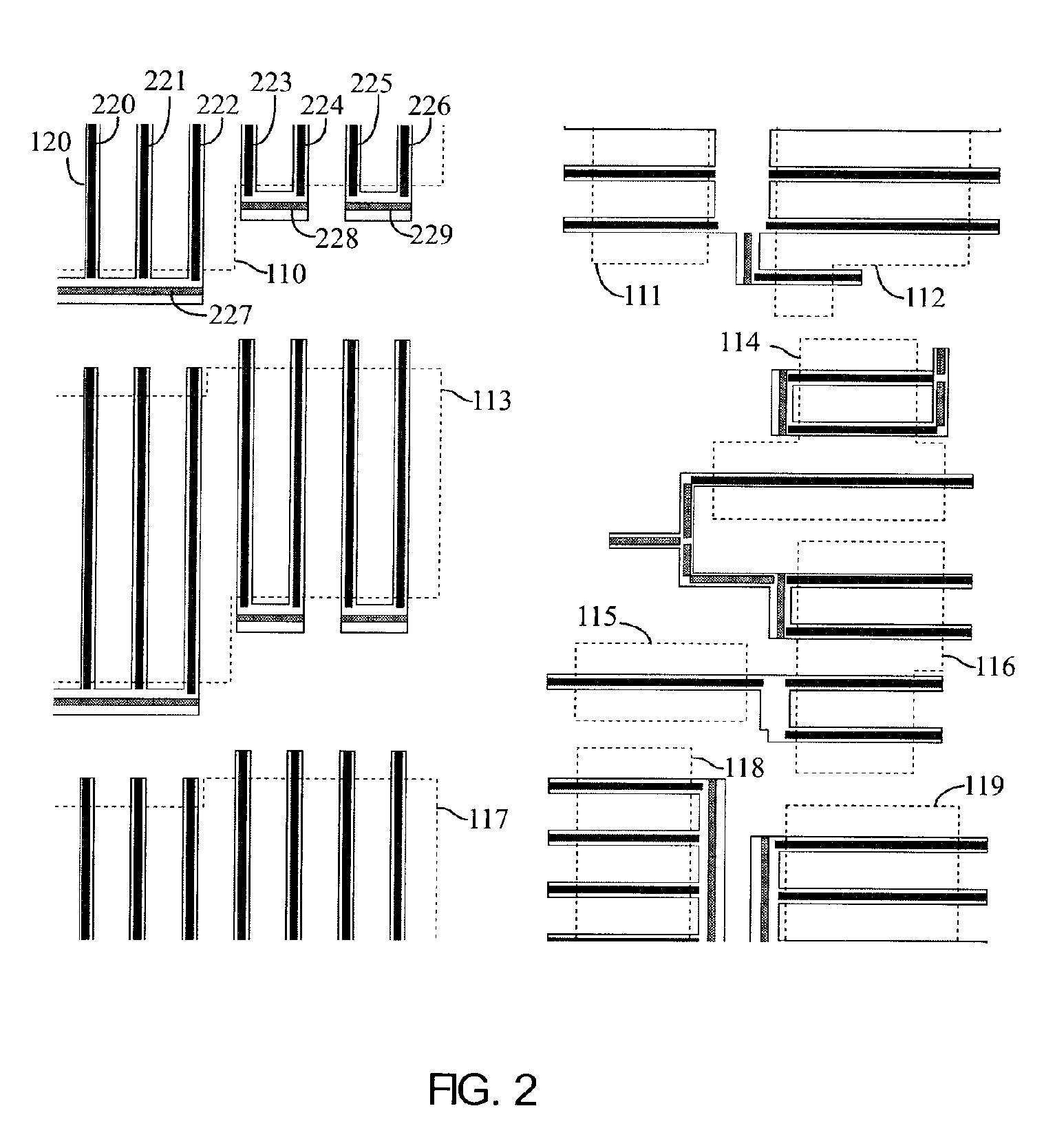
[0039] The invention will now be described with reference to the accompanying figures. In the figures, various aspects of the structures have been shown and schematically represented in a simplified manner to more clearly describe and illustrate the invention.

[0040] By way of overview and introduction, the present invention is directed to a method for conversion of an existing integrated circuit (“IC”) design into a set of masks that optimize use of an edge based image transfer process for fabrication of an IC. An edge based image transfer mask is generated that fabricates an optimized number of edge shapes in the IC pattern. Then a block mask is generated that removes residual sections of the edge based image transfer mask. Finally, a lithography mask is generated for fabrication of any remaining IC shape in the IC pattern that cannot be generated through edge based image transfer. The present invention is a novel method that through an iterative process that selectively creates a...


PUM

PropertyMeasurementUnit
thicknessaaaaaaaaaa
circuit densityaaaaaaaaaa
s wavelengthaaaaaaaaaa

Abstract

The present invention is directed to a method for conversion of an integrated circuit design into a set of masks for fabrication of an integrated circuit that optimizes use of an edge based image transfer mask process.

Description

BACKGROUND OF THE INVENTION [0001] 1. Field of the Invention [0002] The invention relates generally to integrated circuit fabrication and, more particularly, to methods for conversion of an integrated circuit pattern into mask sets that optimize fabrication of said integrated circuit through an edge based pattern transfer process. [0003] 2. Description of the Related Art [0004] The integrated circuit (“IC”) industry strives for electronic devices that are both faster and infinitely smaller. Accordingly, the IC industry is driven by a demand for methods of fabricating IC features with improved dimensional control. IC fabrication with improved dimensional control creates ever smaller IC features, which in turn increases the circuit density of the IC. Increased circuit density yields higher chip performance. Therefore, a substantial economic advantage can be gained through the development of improved methods of fabricating IC features with improved dimensional control. Two prior art IC...

Claims


Application Information

Patent Timeline
Patent Type & Authority Applications(United States)
IPC IPC(8): G06F17/50G06F19/00G03F1/00
CPCG03F1/144G03F1/70
Inventor LIEBMANN, LARS W.BEINTNER, JOCHEN
Owner GOOGLE LLC
Why Eureka
Try Eureka