Nitride semiconductor device and method for manufacturing the same

a technology of semiconductor devices and semiconductors, applied in semiconductor/solid-state device manufacturing, semiconductor devices, electrical equipment, etc., can solve the problems of difficulty in achieving the normally-off-state and high current density in the fet, and achieve the effects of stable characteristics, reduced gate leakage current, and high current operation

Active Publication Date: 2009-08-18
PANASONIC CORP
View PDF7 Cites 60 Cited by
  • Summary
  • Abstract
  • Description
  • Claims
  • Application Information

AI Technical Summary

Benefits of technology

[0019]According to the present invention described above, the gate leakage current is reduced by forming a pn junction in the gate region, thereby achieving a normally-off nitride semiconductor device suitable for high current operation. Further, the nitride semiconductor layers above the channel are prevented from variations in thickness by providing the p-type nitride semiconductor layer on the nitride semiconductor layer in the gate region. This makes it possible to provide the nitride semiconductor device with stable characteristics such as high current density, low leakage current and high breakdown voltage, thereby improving productivity.

Problems solved by technology

Therefore, it has been difficult to achieve both of the normally-off state and high current density in the FET.

Method used


Image

  • Nitride semiconductor device and method for manufacturing the same
  • Nitride semiconductor device and method for manufacturing the same
  • Nitride semiconductor device and method for manufacturing the same

Examples


first embodiment

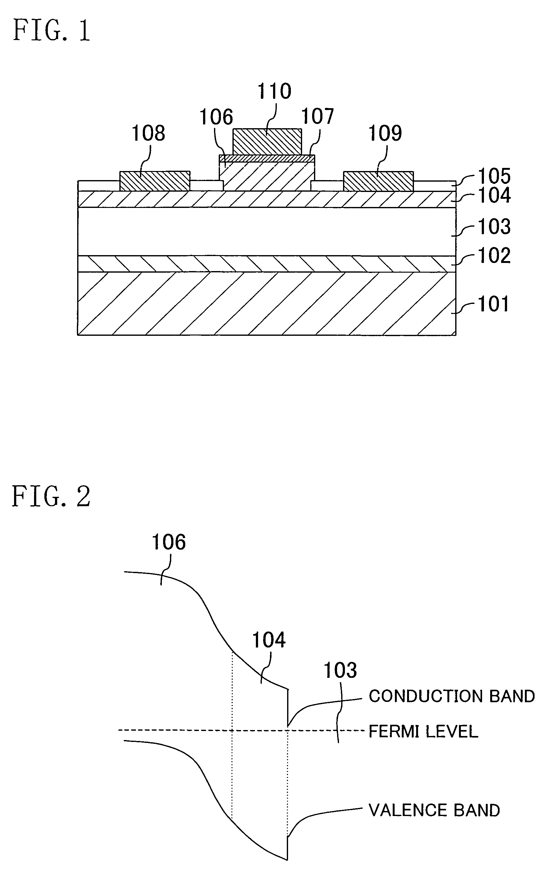
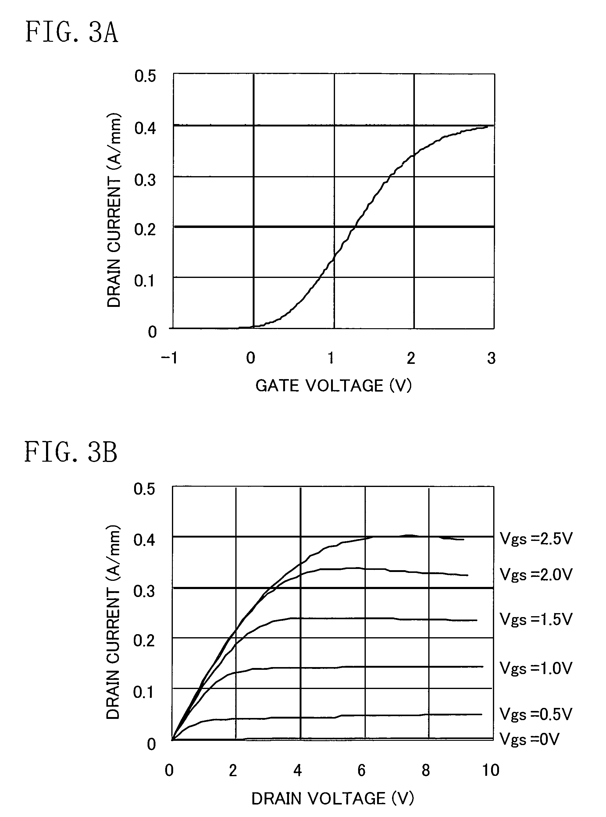
[0029]FIG. 1 is a sectional view illustrating a nitride semiconductor device according to a first embodiment of the present invention. The nitride semiconductor device of the present embodiment is a field effect transistor used as a power transistor.

[0030]As shown in FIG. 1, the nitride semiconductor device of the present embodiment includes a sapphire substrate 101 having a (0001) plane as a principle surface, a 100 nm thick AlN buffer layer 102 formed on the (0001) plane of the sapphire substrate 101, a 2 μm thick undoped GaN layer 103 formed on the AlN buffer layer 102, a 25 nm thick undoped AlGaN layer 104 formed on the undoped GaN layer 103, a 100 nm thick p-AlGaN layer 106 formed on part of the undoped AlGaN layer 104 and a 5 mm thick high concentration p-GaN layer 107 formed on the p-AlGaN layer 106. The term “undoped” means that impurities are not intentionally introduced into the layer.

[0031]The p-AlGaN layer 106 is doped with Mg at a concentration of about 1×1019 cm−3 and ...

second embodiment

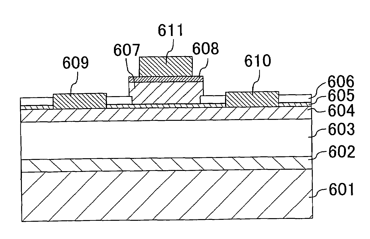
[0054]FIG. 6 is a sectional view illustrating a nitride semiconductor device according to a second embodiment of the present invention.

[0055]As shown in FIG. 6, the nitride semiconductor device of the present embodiment includes a sapphire substrate 601 having a (0001) plane as a principle surface. On the (0001) plane of the sapphire substrate 601, a 100 nm thick AlN buffer layer 602, a 2 μm thick undoped GaN layer 603, a 25 nm thick undoped AlGaN layer 604, a 5 nm thick first p-AlGaN layer 605 doped with Mg, a 100 nm thick second p-AlGaN layer 607 doped with Mg and a 5 nm thick high concentration p-GaN layer 608 are formed in this order. The undoped AlGaN layer 604, the first p-AlGaN layer 605 and the second p-AlGaN layer 607 are made of Al0.2Ga0.8N, for example. The first p-AlGaN layer 605 and the second p-AlGaN layer 607 are doped with Mg at a concentration of about 1×1019 cm−3, respectively.

[0056]The nitride semiconductor device of the present embodiment further includes a gate ...


PUM


Abstract

An AlN buffer layer, an undoped GaN layer, an undoped AlGaN layer, a first p-AlGaN layer, a second p-AlGaN layer and a high concentration p-GaN layer are formed in this order on a substrate. A gate electrode establishes ohmic contact with the high concentration p-GaN layer. A source electrode and a drain electrode are formed on the undoped AlGaN layer. Two-dimensional electron gas generated at the interface between the undoped AlGaN layer and the undoped GaN layer and the first and second p-AlGaN layers form a pn junction in a gate region. The second p-AlGaN layer covers a SiN film in part.

Description

BACKGROUND OF THE INVENTION[0001]1. Field of the Invention[0002]The present invention relates to nitride semiconductor devices applicable to power transistors for use in power supply circuits of consumer products, such as television sets.[0003]2. Description of Related Art[0004]In recent years, active research and development have been made on the application of field effect transistors (hereinafter referred to as FETs) using a GaN-based material to high-frequency and high-power devices. Nitride semiconductor materials such as GaN are capable of producing various kinds of mixed crystal such as AlN and InN, as well as heterojunction just like conventionally used arsenic semiconductor materials such as GaAs. At the heterojunction interface between nitride semiconductor layers, high concentration carriers are generated by spontaneous or piezoelectric polarization without injecting any dopants. Therefore, if the nitride semiconductor material is used, the resulting FET is likely to be a...

Claims


Application Information

Patent Timeline
Patent Type & Authority Patents(United States)
IPC IPC(8): H01L31/072
CPCH01L29/7787H01L29/66462H01L29/1066H01L29/2003H01L29/432
Inventor HIKITA, MASAHIROYANAGIHARA, MANABUUEDA, TETSUZOUEMOTO, YASUHIROTANAKA, TSUYOSHI
Owner PANASONIC CORP
Why Eureka
Try Eureka