Electrical interconnect structure and process thereof and circuit board structure

Inactive Publication Date: 2009-11-19
UNIMICRON TECH CORP
View PDF18 Cites 4 Cited by
  • Summary
  • Abstract
  • Description
  • Claims
  • Application Information

AI Technical Summary

Benefits of technology

[0038]In light of the foregoing, the ultra fine pattern is inlaid in the surface of the core and is partially connected to the patterned conductive layer located on the surf

Problems solved by technology

However, owing to the limitation on the line width and the pitch of ultra fine wires, the layout density of the circuit board is not able to be further enhanced.
Therefore, when the circuits are prone to be equipped with high density and

Method used


Image

  • Electrical interconnect structure and process thereof and circuit board structure
  • Electrical interconnect structure and process thereof and circuit board structure
  • Electrical interconnect structure and process thereof and circuit board structure

Examples


first embodiment

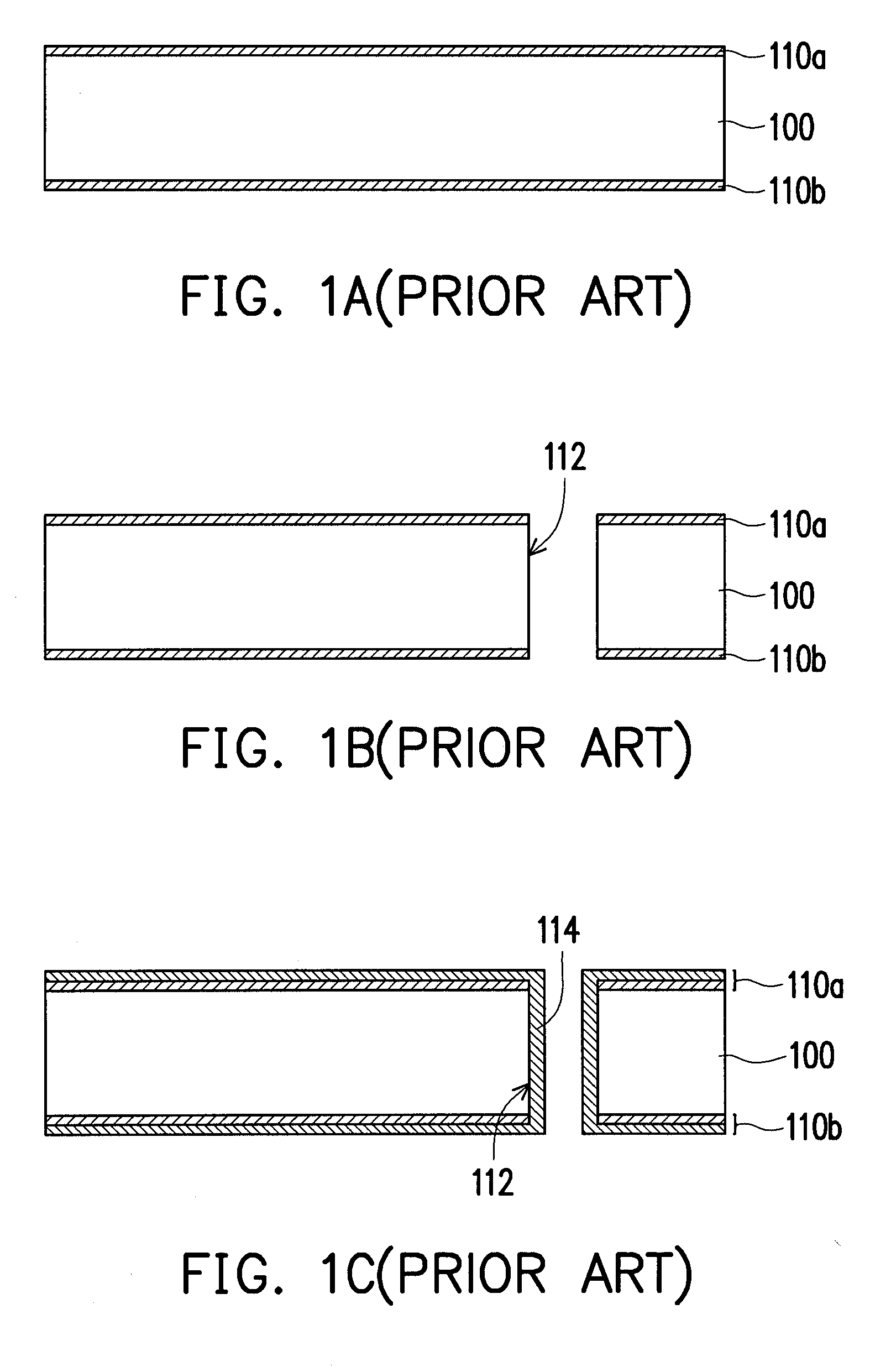
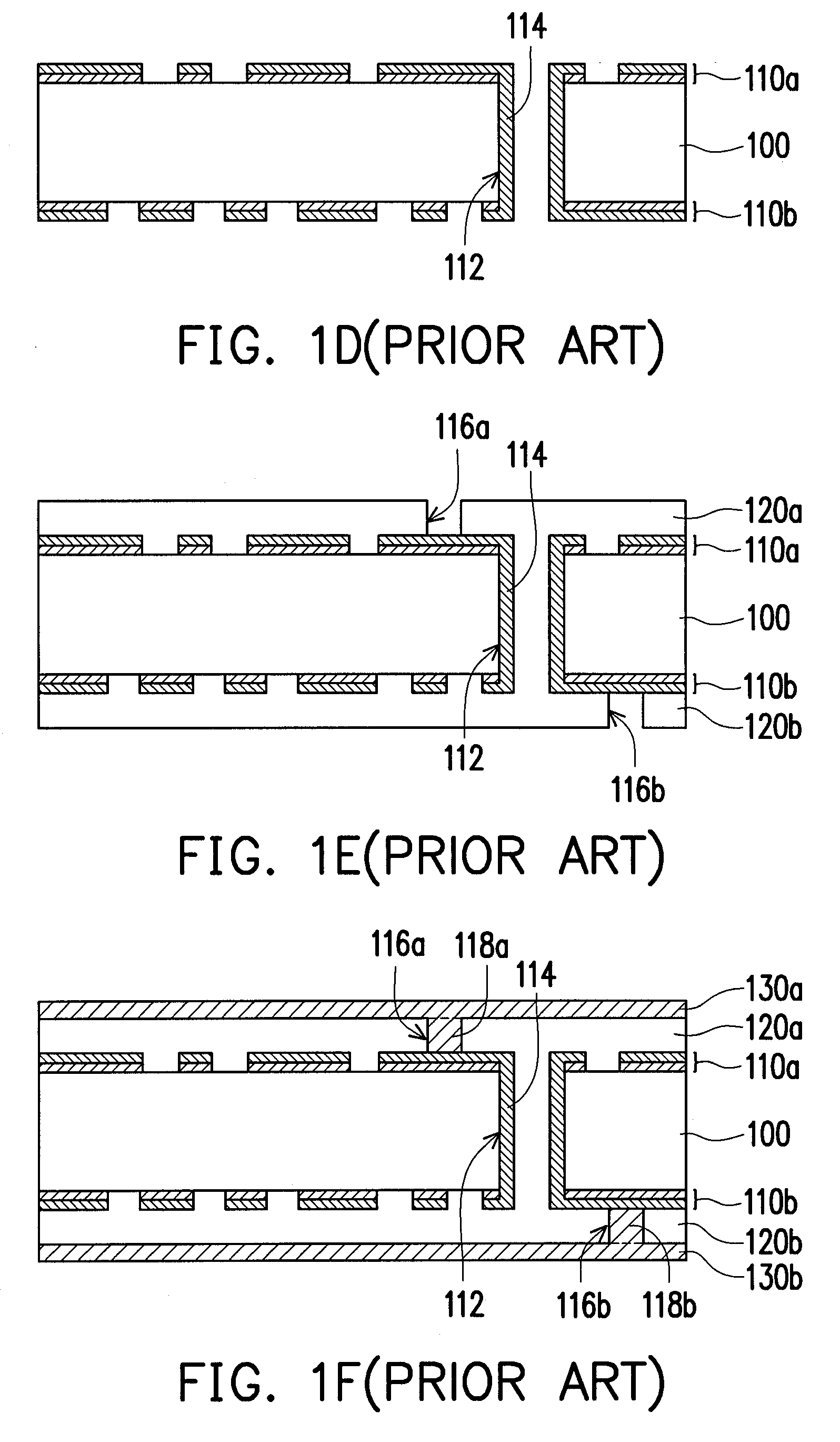
[0045]The first embodiment teaches a circuit board having two conductive layers. Please refer to FIGS. 2A through 2E which are cross-sectional flowcharts of a process for fabricating an electrical interconnecting structure according to the first embodiment of the present invention.

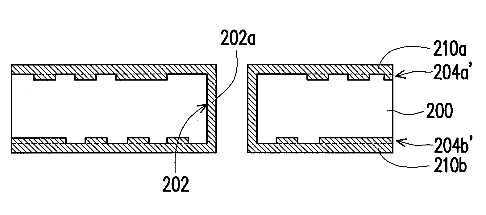
[0046]As shown in FIG. 2A, a plate to be used in the process for fabricating the electrical interconnecting structure can be a double-sided plate in which two conductive layers are respectively disposed on two sides of a single dielectric layer, an one-sided plate in which a conductive layer is disposed on one side of a single dielectric layer, or a single dielectric layer. In the present embodiment, a core 200 is a single dielectric layer made of epoxy resin or glass-fiber-containing epoxy resin.

[0047]With reference to FIG. 2B, based on the required circuit layout, at least a through hole 202 is formed in the core 200 by way of mechanical drilling or laser ablating, for example. In the meantime, an ultra ...

second embodiment

[0052]In comparison with the first embodiment in which the circuit board is equipped with two conductive layers, the second embodiment teaches a circuit board having four conductive layers. Please refer to FIGS. 3A through 3I which are cross-sectional flowcharts of a process for fabricating an electrical interconnecting structure according to the second embodiment of the present invention.

[0053]As shown in FIG. 3A, a plate to be used in the process for fabricating the electrical interconnecting structure can be a double-sided plate in which two conductive layers are respectively disposed on two sides of a single dielectric layer, an one-sided plate in which a conductive layer is disposed on one side of a single dielectric layer, or a single dielectric layer. In the present embodiment, the circuit board acting as a core 300 of the plate to be used in the process for fabricating the electrical interconnecting structure is referred to as the double-sided plate. The core 300 may include...

third embodiment

[0063]Please refer to FIGS. 4A through 4J which are cross-sectional flowcharts of a process for fabricating an electrical interconnecting structure according to a third embodiment of the present invention.

[0064]As shown in FIG. 4A, a plate to be used in the process for fabricating the electrical interconnecting structure can be a double-sided plate in which two conductive layers are respectively disposed on two sides of a single dielectric layer, an one-sided plate in which a conductive layer is disposed on one side of a single dielectric layer, or a single dielectric layer. In the present embodiment, the circuit board acting as a core 400 of the plate to be used in the process for fabricating the electrical interconnecting structure is referred to as the double-sided plate. The core400 may include a dielectric layer 410 and two conductive layers 412a and 412b to be patterned. Here, the dielectric layer 410 can be made of epoxy resin or glass-fiber-containing epoxy resin. The conduc...


PUM

PropertyMeasurementUnit
Dielectric polarization enthalpyaaaaaaaaaa
Electrical conductoraaaaaaaaaa

Abstract

An electrical interconnecting structure suitable for a circuit board is provided. The electrical interconnecting structure includes a core, an ultra fine pattern, and a patterned conductive layer. The core has a surface, and the ultra fine pattern is inlaid in the surface of the core. The patterned conductive layer is disposed on the surface of the core and is partially connected to the ultra fine pattern. Since the ultra fine pattern of the electrical interconnecting structure is inlaid in the surface of the core and is partially connected to the patterned conductive layer located on the surface of the core.

Description

CROSS-REFERENCE TO RELATED APPLICATION[0001]This application claims the priority benefit of Taiwan application serial no. 97117559, filed on May 13, 2008. The entirety of the above-mentioned patent application is hereby incorporated by reference herein and made a part of specification.BACKGROUND OF THE INVENTION[0002]1. Field of the Invention[0003]The present invention is related to an electrical interconnecting structure. More particularly, the present invention is related to an electrical interconnecting structure applied to a circuit board and a fabricating process thereof.[0004]2. Description of Related Art[0005]A conventional circuit board is mainly composed of a plurality of patterned conductive layers and a plurality of dielectric layers alternately stacked to one another. In addition, the patterned conductive layers are electrically connected through a plurality of conductive vias. On the other hand, the circuit board can be further categorized by processes for fabricating t...

Claims


Application Information

Patent Timeline
IPC IPC(8): H01R9/00H05K1/14H05K1/11
CPCH05K1/0265H05K3/0032H05K3/0038H05K3/107H05K3/426Y10T29/49147H05K3/4602H05K3/465H05K3/4652H05K2201/09536H05K2201/09736H05K3/428
Inventor CHEN, TSUNG-YUANCHIANG, SHU-SHENGCHENG, DAVID C. H.
Owner UNIMICRON TECH CORP
Why Eureka
Try Eureka