Manufacturing method for multi-layer circuit board

a manufacturing method and multi-layer technology, applied in the direction of resistive material coating, nuclear engineering, railway components, etc., can solve the problems of inability to miniaturize the design of conductive holes and bonding pads on the bottom layer, and the alignment errors caused by the alignment targets of each layer continuously accumulate, so as to improve the interlayer alignment accuracy of the multi-layer circuit board and increase the wiring density of the circuit layer

Inactive Publication Date: 2015-05-07
UNIMICRON TECH CORP
View PDF3 Cites 2 Cited by
  • Summary
  • Abstract
  • Description
  • Claims
  • Application Information

AI Technical Summary

Benefits of technology

[0006]The invention provides a manufacturing method for a multi-layer circuit board capable of improving an interlayer alignment accuracy of the multi-layer circuit board, increasing a wiring density of a circuit layer, making it possible that conductive holes and bonding pads on bottom layers are designed to be miniaturized owing to the alignment accuracy. Even a pattern design with a single-side alignment accuracy up to less than 50 μm may be achieved.

Problems solved by technology

However, since the alignment targets in the previous stacking layer are formed through the photolithography process, the process itself already causes errors.
When the milling process using X ray is performed, additional errors in the milling process also occur.
Thus, alignment errors caused by the alignment targets of each layer continuously accumulate.
If a number of circuit layers of the circuit board increases, the accumulated errors of the alignment targets also increase, resulting in an overly large deviation of an interlayer alignment accuracy that makes a design of conductive holes and bonding pads on bottom layers unable to be miniaturized.

Method used


Image

  • Manufacturing method for multi-layer circuit board
  • Manufacturing method for multi-layer circuit board
  • Manufacturing method for multi-layer circuit board

Examples


Embodiment Construction

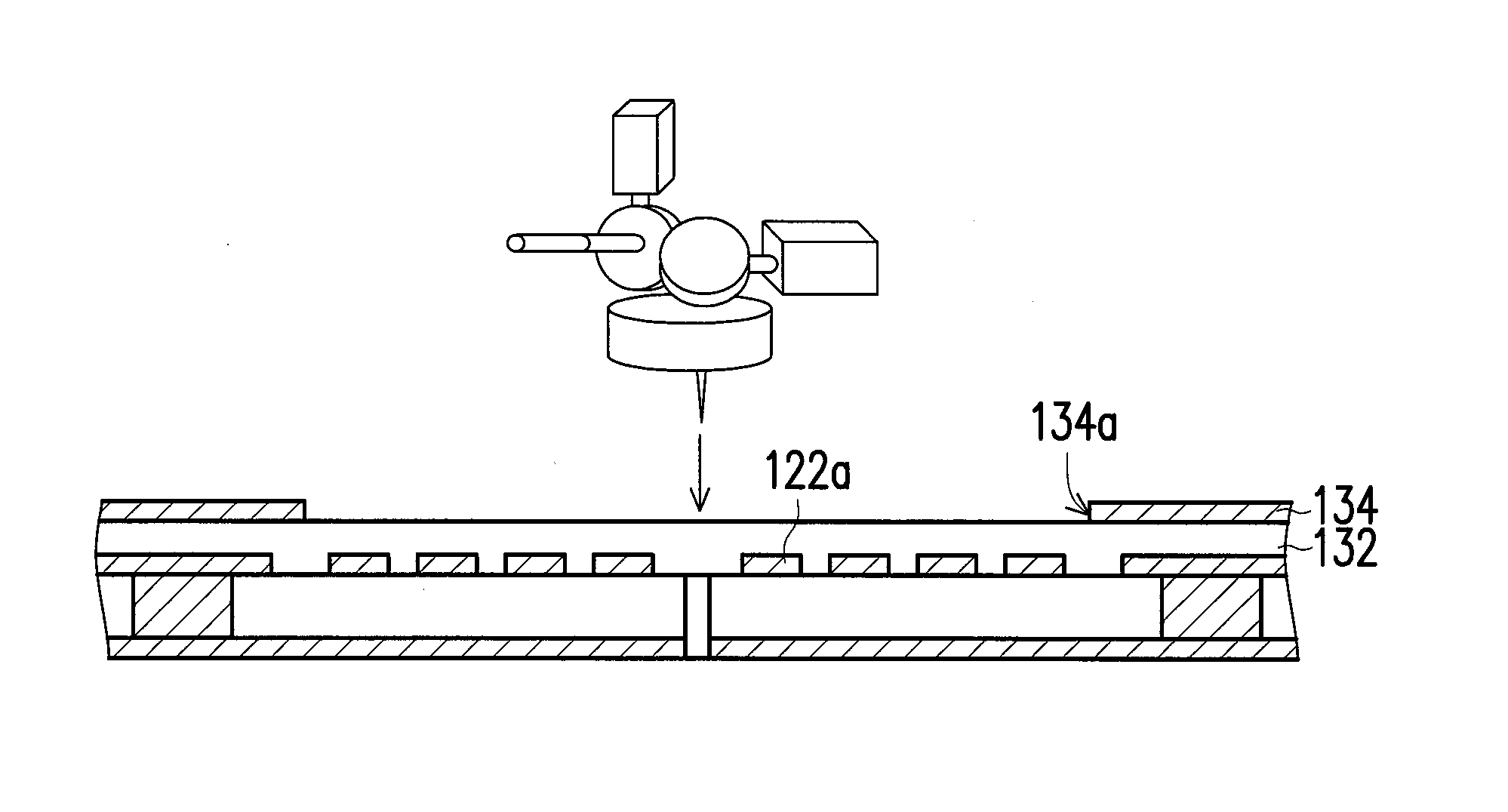
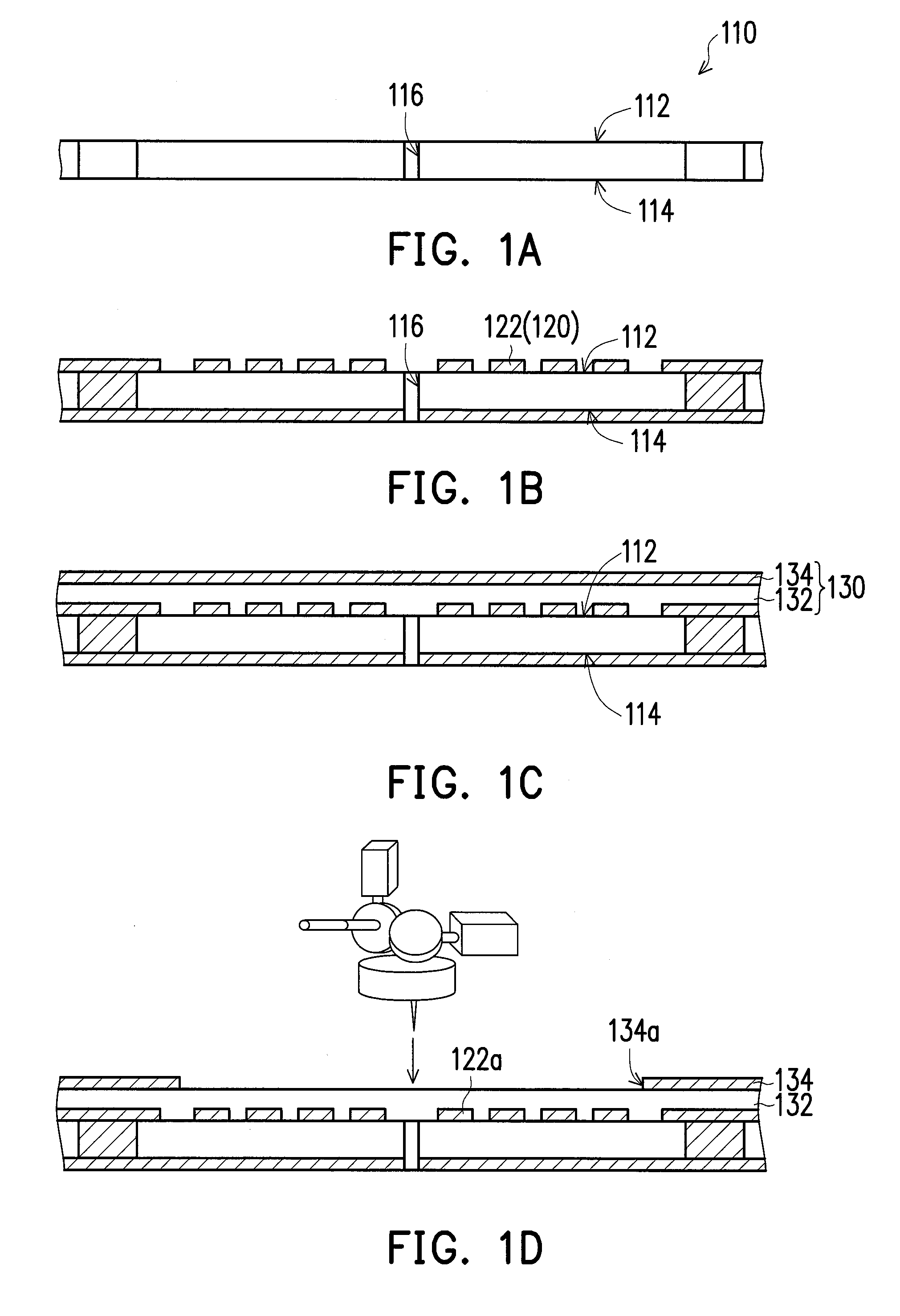
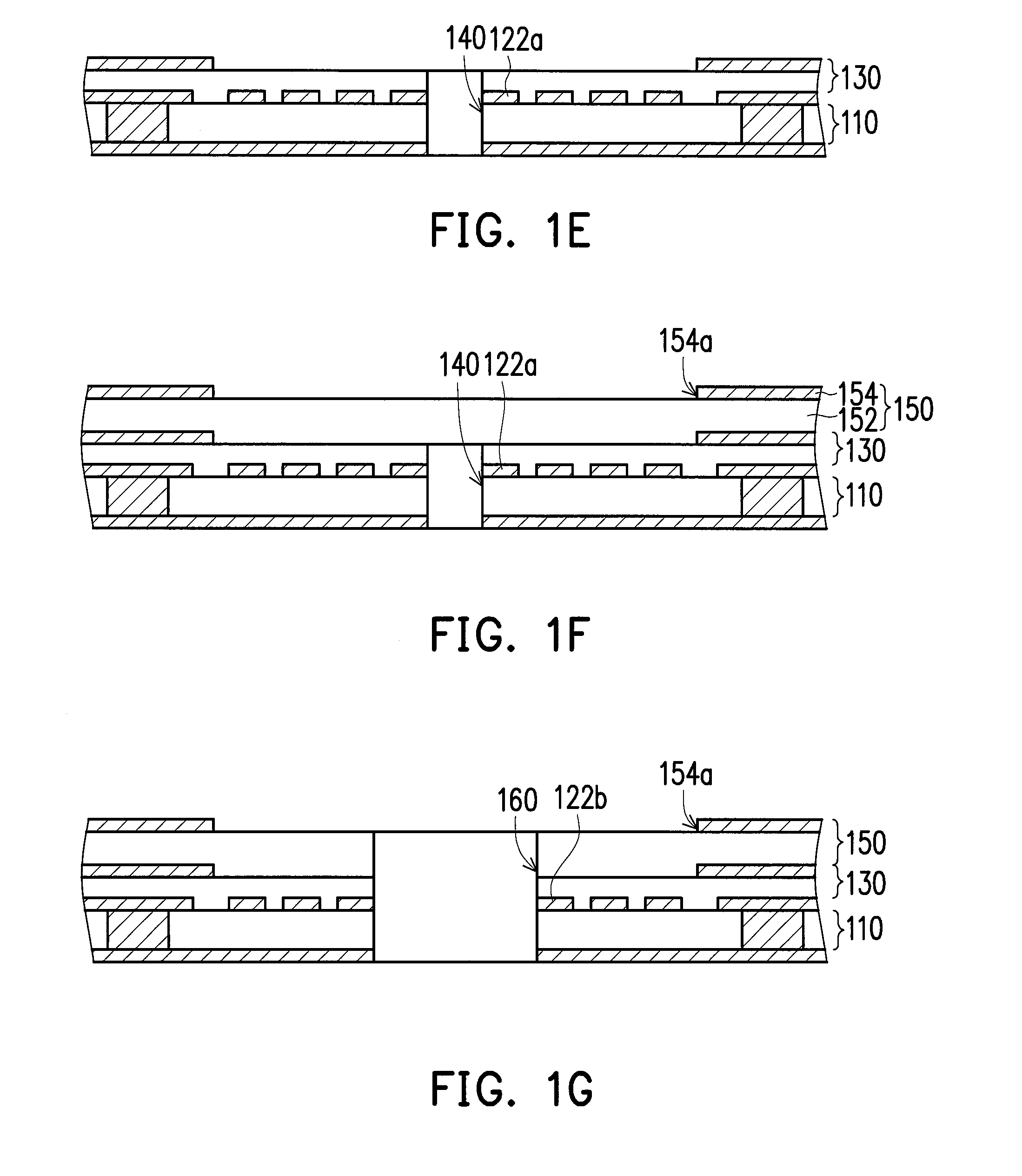
[0016]FIGS. 1A to 1G are schematic views illustrating a process flow of a manufacturing method for a multi-layer circuit board according to an embodiment of the invention. FIG. 2 is a schematic top view of a substrate and a first patterned circuit layer according to an embodiment of the invention. In the present embodiment, the manufacturing method for the multi-layer circuit board includes the following. First, as shown in FIG. 1A, a substrate 110 is provided. The substrate 110 includes two surfaces 112 and 114 opposite to each other and a first via 116 penetrating the substrate 110. Then, referring to FIG. 1B and FIG. 2 together, a first patterned circuit layer 120 is formed on the surface 112 by using the first via 116 as an alignment target. In the present embodiment, as shown in FIG. 2, an outer diameter D1 of the first via 116 substantially ranges between 0.5 mm and 0.8 mm. It should be noted that, a manufacturing process illustrated in FIG. 1A to FIG. 1G are cross-sectional v...


PUM

PropertyMeasurementUnit
outer diameter D1aaaaaaaaaa
infrared wavelength rangeaaaaaaaaaa

Abstract

A manufacturing method for a multi-layer circuit board includes the following steps. Firstly, a substrate having a first via penetrating the substrate is provided. Next, a patterned circuit layer is formed on a surface of the substrate by using the first via as an alignment target. The first patterned circuit layer includes a first concentric-circle pattern surrounding the first via. Next, a first stacking layer is formed on the surface. Then, a first through hole penetrating regions where a first concentric circle from the center of the concentric-circle pattern is orthogonally projected on the first stacking layer and the substrate is formed. Next, a second stacking layer is formed on the first stacking layer. Afterward, a second through hole penetrating regions where a second concentric circle from the center of the concentric-circle pattern is orthogonally projected on of the first, the second stacking layers and the substrate is formed.

Description

BACKGROUND OF THE INVENTION[0001]1. Field of the Invention[0002]The invention relates to a manufacturing method for a circuit board, and particularly relates to a manufacturing method for a multi-layer circuit board.[0003]2. Description of Related Art[0004]As the integration of electronic products is increasingly improved, a circuit layer of a circuit board applied to the high-integration electronic products increases from single layer, double layer to 6 layers, 8 layers and even more than 10 layers, so as to mount more electronic components on a printed circuit board. Generally speaking, the most common manufacturing process for a circuit board is the lamination process. When the lamination process is used to manufacture the circuit board, an alignment accuracy between each circuit layer and insulating layer needs to be appropriately controlled. Therefore, in the manufacturing process of the circuit board, a plurality of alignment targets are usually formed in a previous stacking l...

Claims


Application Information

Patent Timeline
Patent Type & Authority Applications(United States)
IPC IPC(8): H05K3/46H05K3/10H05K3/00
CPCH05K3/46H05K3/244H05K1/111H05K3/40B05D5/12H05K3/10B05D7/50H05K3/12H05K1/0298H05K3/4644H05K3/0047C23C18/165H05K1/0269H05K3/0038H05K3/4679H05K2203/1476
Inventor HUANG, PEI-CHANGYU, CHENG-POHUANG, HAN-PEI
Owner UNIMICRON TECH CORP
Why Eureka
Try Eureka