

Method for fabricating circuit board structure
- Summary
- Abstract
- Description
- Claims
- Application Information
AI Technical Summary
Benefits of technology
Problems solved by technology
Method used
Image

Examples
first embodiment
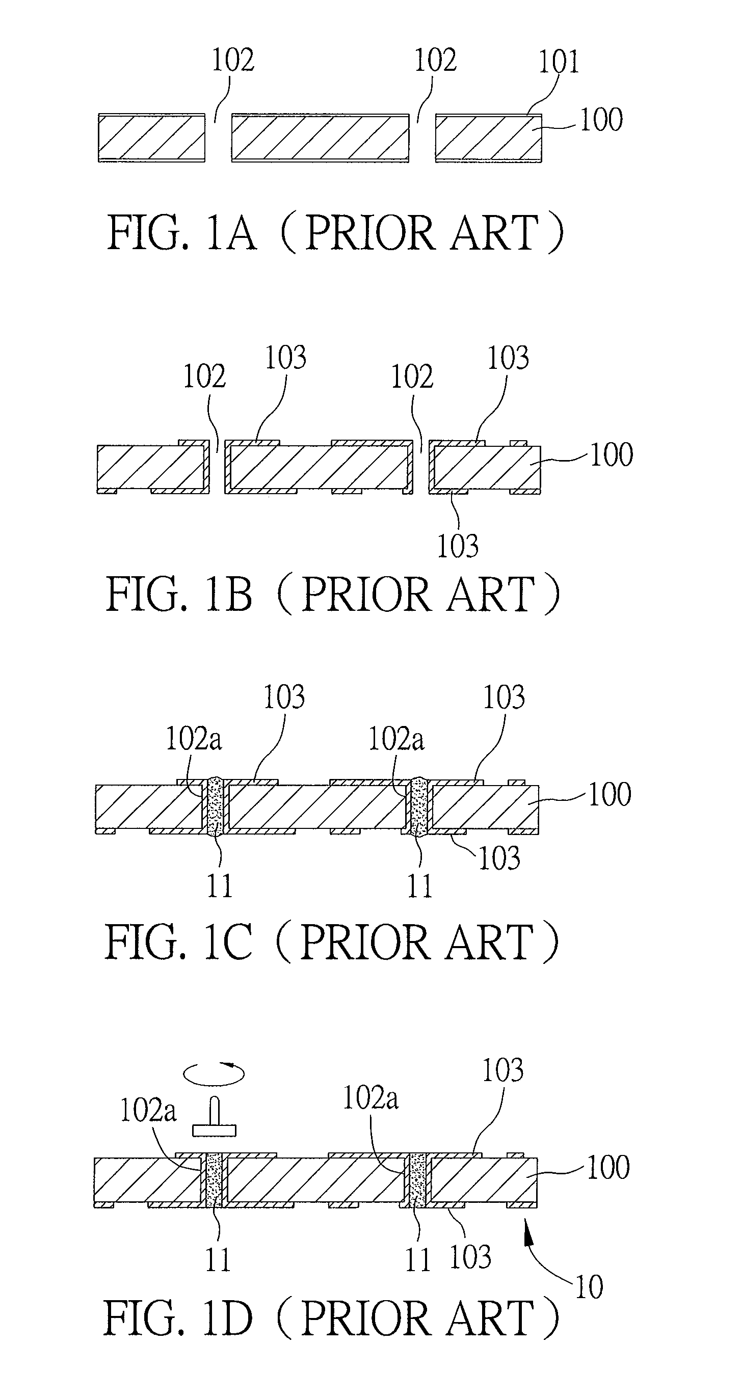
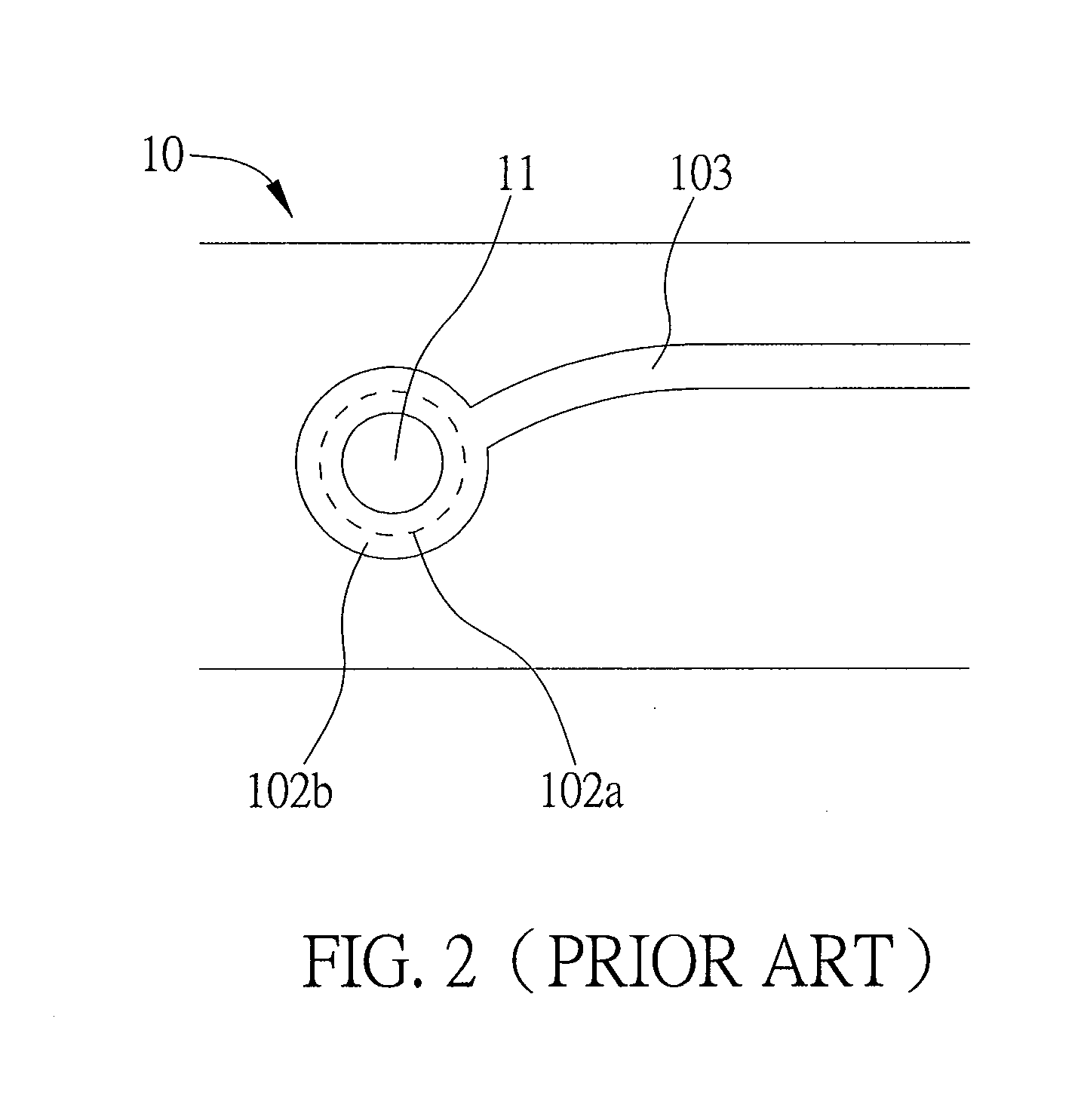
[0036]FIGS. 3A to 3D are sectional diagrams showing a method for fabricating a circuit board structure according to a first embodiment of the present invention.
[0037]As shown in FIG. 3A, a carrier board 21 having a first surface 21a and a second surface 21b is provided. The carrier board 21 can be one of a dielectric board, a copper clad laminate, a double-layer circuit board and a multi-layer circuit board. The prevent invention exemplifies a carrier board 21 of copper clad laminate, but it is not limited thereto. The first surface 21a and the second surface 21b of the carrier board 21 are respectively disposed with copper foil 211. At least a through hole 210 is formed in the carrier board 21 and penetrating the first surface 21a and the second surface 21b.
[0038]Alternatively, as shown in FIG. 3A′, a roughening process is performed to roughen the first surface 21a and the second surface 21b as well as surface of the through hole 210 of the carrier board 21 and meanwhile the coppe...
second embodiment
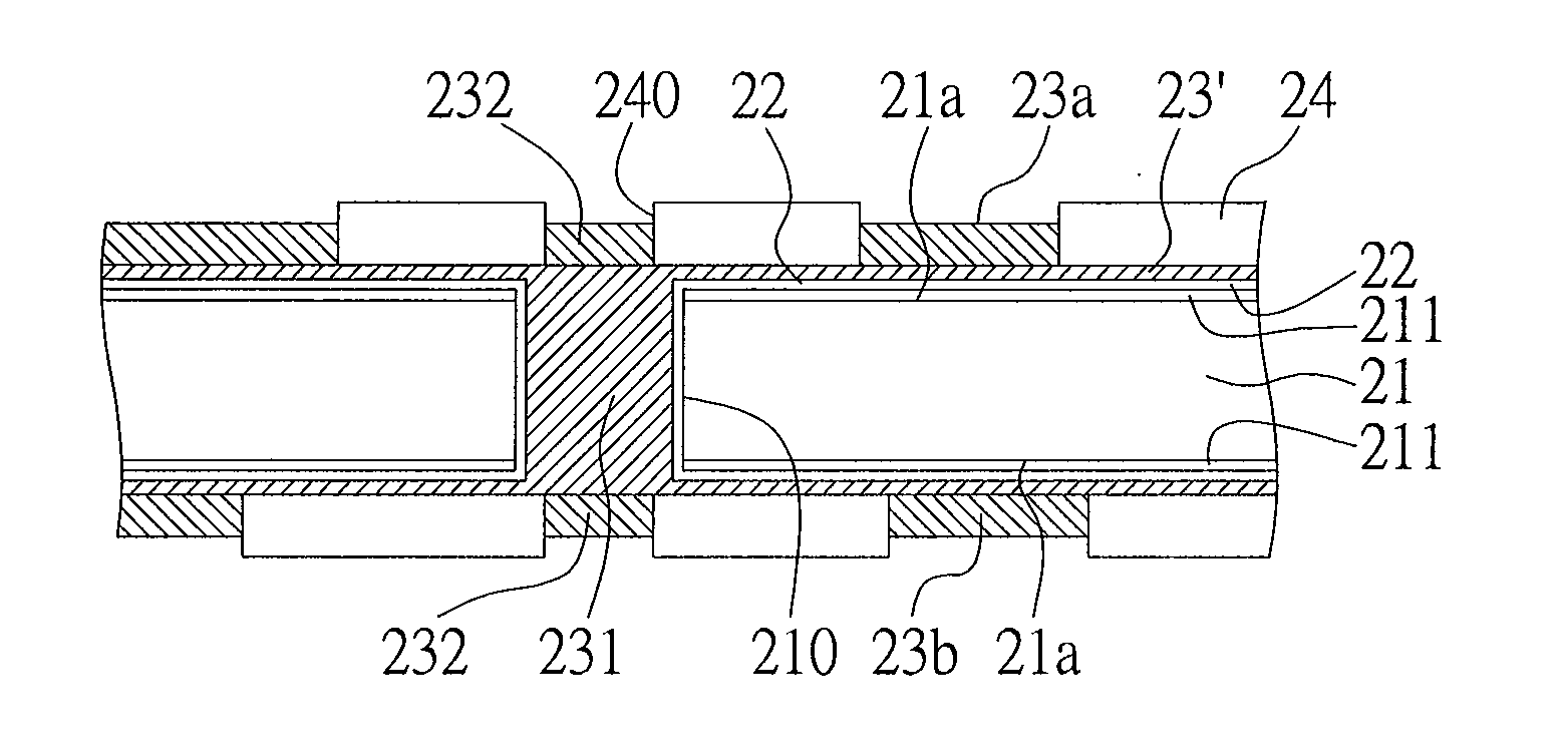
[0044]FIGS. 5A to 5E are sectional diagrams showing a method for fabricating a circuit board structure according to a second embodiment of the present invention. A main difference of the present embodiment from the first embodiment is the circuit of the first and second circuit layers on surfaces of the carrier board is electrically connected to top surface of the end portions of the conductive pillar.
[0045]As shown in FIG. 5A, as a continuation of the process of FIG. 3B in the first embodiment, a metal layer 23 is formed on the conductive layer 22 on the first and second surfaces 21a, 21b of the carrier board 21 and a conductive pillar 231 is formed in the through hole 210 of the carrier board 21 by electroplating.
[0046]As shown in FIG. 5B, the metal layer 23 on the first and second surfaces 21a, 21b of the carrier board 21 is thinned so as to form a thin metal layer 23′.
[0047]As shown in FIG. 5C, a resist layer 24 is formed on surface of the thin metal layer 23′ and a plurality of...
third embodiment
[0052]FIGS. 7A to 7F are sectional diagrams showing a method for fabricating a circuit board structure according to a third embodiment of the present invention. Different from the first and second embodiments, the first and second circuit layers of the present embodiment are electrically connected to the two ends of the conductive pillar through a conductive layer.
[0053]As shown in FIG. 7A, as a continuation of the process of FIG. 3B, a metal layer 23 is formed on the conductive layer 22 on the first and second surfaces 21a, 21b of the carrier board 21 and a conductive pillar 231 is formed in the through hole 210 of the carrier board 21 by electroplating.
[0054]As shown in FIG. 7B, the metal layer 23, the conductive layer 22 and the copper foil 211 on the first and second surfaces 21a, 21b are removed.
[0055]As shown in FIG. 7C, another conductive layer 22′ is formed on the first surface 21a, the second surface 21b and the two ends of the conductive pillar 231 of the carrier board 21....
PUM
| Property | Measurement | Unit |
|---|---|---|
| Diameter | aaaaa | aaaaa |
| Density | aaaaa | aaaaa |
| Electrical conductor | aaaaa | aaaaa |
Abstract
Description
Claims
Application Information