
Mold for nano-imprinting and method of manufacturing the same

a nano-imprinting and mold technology, applied in the field of molds for nano-imprinting and a manufacturing method, can solve the problems of difficult manufacturing of nano-imprint molds, irregular imprint formation, hard molds made of quartz or glass, etc., and achieve the effect of preventing damage and improving durability

Inactive Publication Date: 2008-03-13
SAMSUNG ELECTRONICS CO LTD
View PDF7 Cites 48 Cited by
  • Summary
  • Abstract
  • Description
  • Claims
  • Application Information

AI Technical Summary

Benefits of technology

[0007]Accordingly, exemplary embodiments of the present invention have been made to address the above-mentioned problems occurring in the prior art, and it is an aspect of the present invention to provide a mold for nano-imprinting, which can be manufactured by uniformly replicating an original pattern on a substrate having an irregular surface, and have an improved durability, so that damage thereto can be prevented.
[0008]It is another aspect of the present invention to provide a method for easily manufacturing a nano-imprint mold.

Problems solved by technology

However, since the nano-imprint mold using quartz or glass is made through a dry-etching process after a lithography process, it is difficult to manufacture the nano-imprint mold.
Further, the mold made of quartz or glass is hard.
Therefore, if a substrate on which a pattern is carved has an irregular surface, the contact between the mold and substrate is irregular, and thereby causes the imprint to be irregularly formed.
Further, the irregular surface of the substrate can damage the mold used for the imprint.
However, there is a problem in that a nano-pattern can be damaged and deformed in an imprint process due to the flexibility of the mold.

Method used


Image

  • Mold for nano-imprinting and method of manufacturing the same
  • Mold for nano-imprinting and method of manufacturing the same
  • Mold for nano-imprinting and method of manufacturing the same

Examples


Embodiment Construction

[0019]Hereinafter, the present invention will be described in detail with reference to the accompanying drawings.

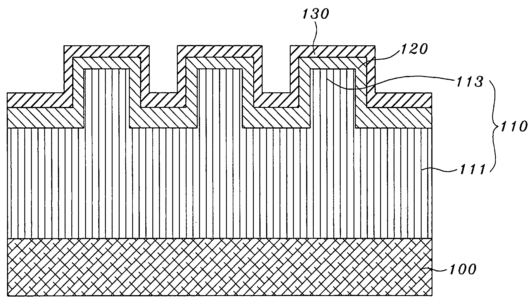
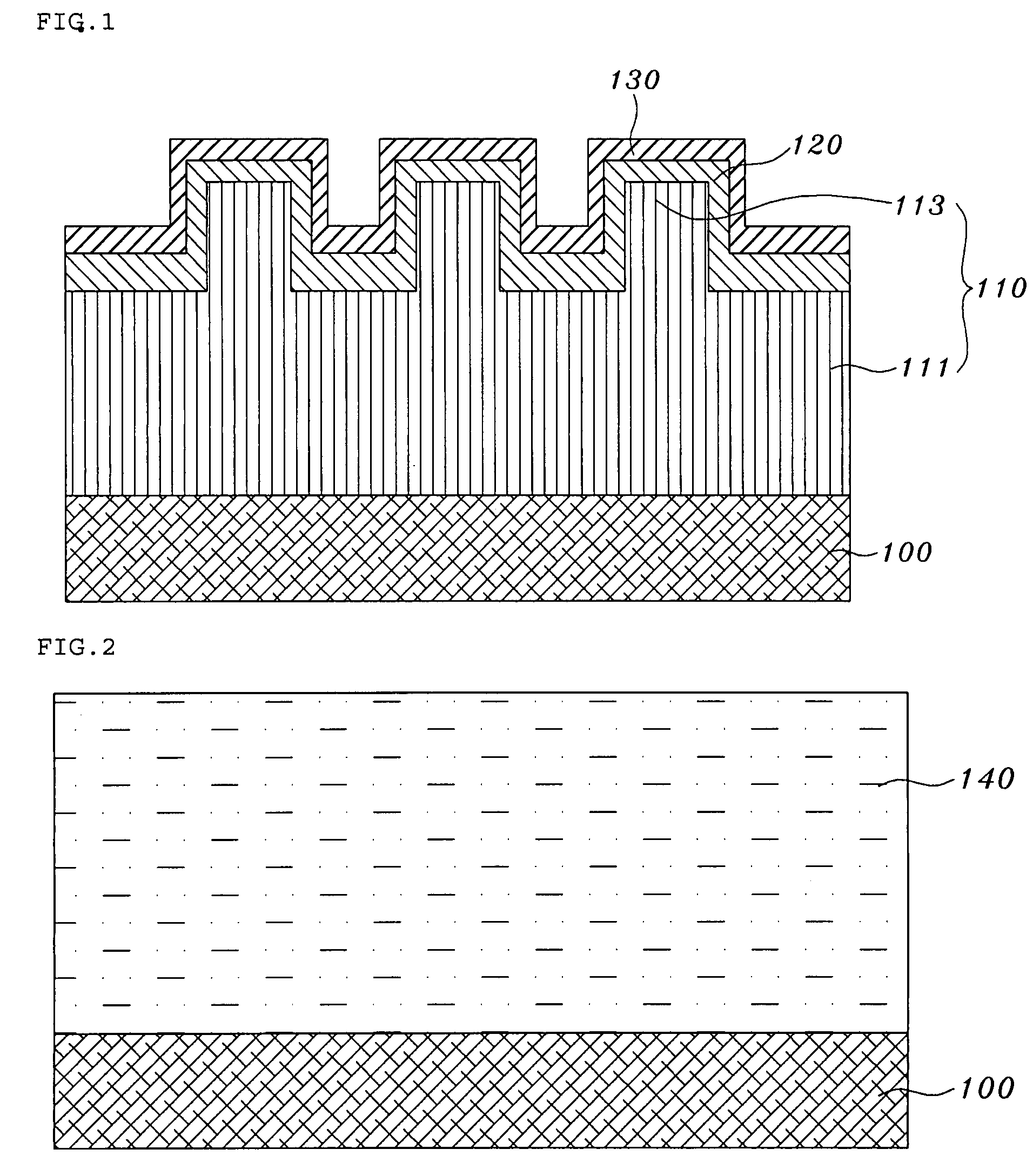
[0020]FIG. 1 is a sectional view showing a nano-imprint mold according to an exemplary embodiment of the present invention.

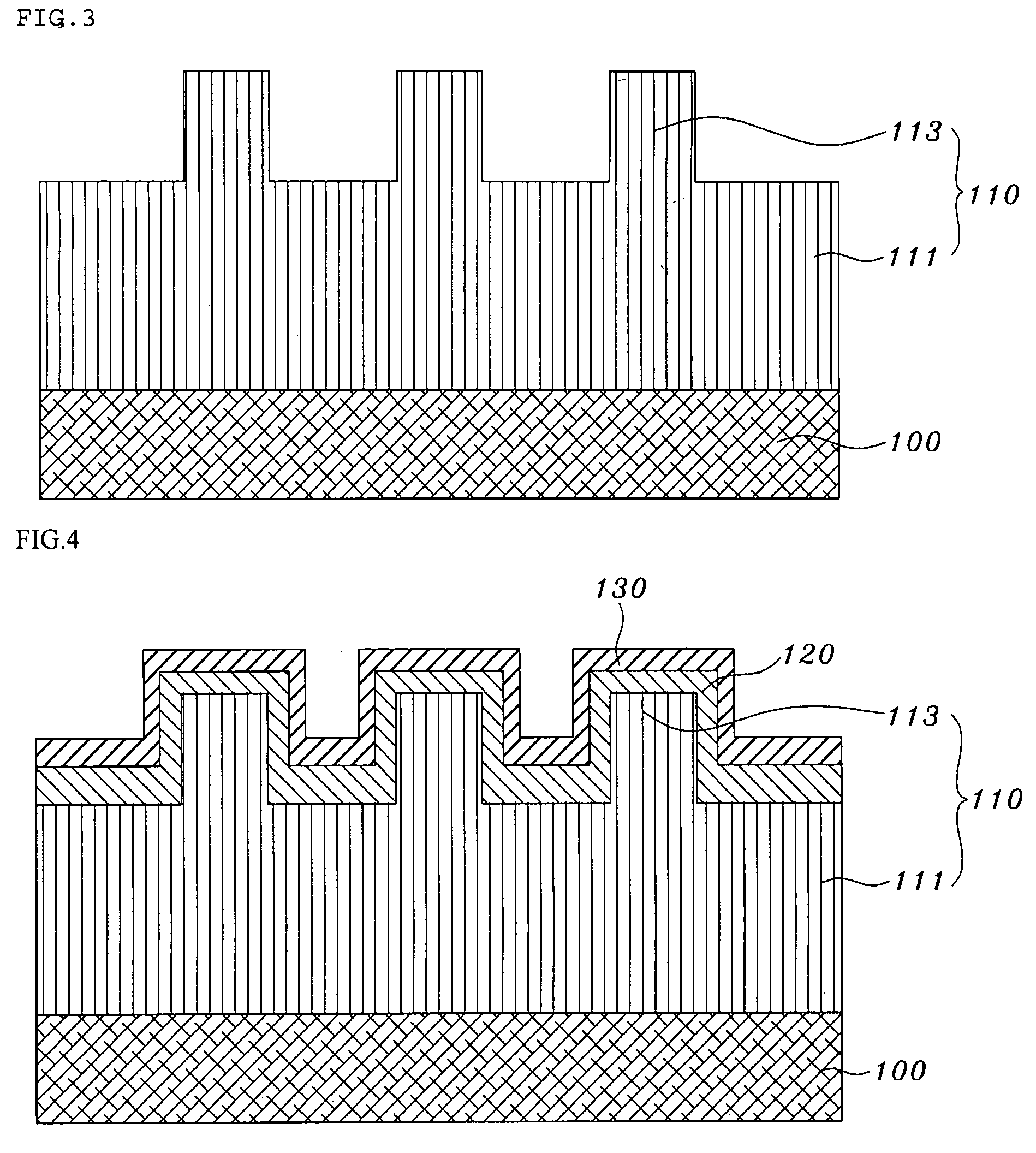
[0021]As shown in FIG. 1, the nano-imprint mold consistent with the present invention comprises a substrate 100, a pattern portion 110 formed on the substrate 100 and provided with a prominence and depression pattern 113, a hard layer 120 formed on a surface of the pattern portion 110, and a separation layer 130 formed on a surface of the hard layer 120.

[0022]The substrate 100 supports the pattern portion 110 formed on an upper portion of the substrate 100, and preferably, but not necessarily, is made of hard materials such as quartz or glass or soft materials such as Polyethylene Terephthalate (PET) and Polycarbonate (PC), through which ultraviolet rays can be transmitted.

[0023]The pattern portion 110 comprises a buffer layer 111 formed on an entire ...


PUM

PropertyMeasurementUnit
Pressureaaaaaaaaaa
Structureaaaaaaaaaa
Hardnessaaaaaaaaaa

Abstract

A nano-imprint mold and a method of manufacturing the same are provided, which can be used for replicating a nano-scaled structure to a polymer layer. The nano-imprint mold comprises: a substrate; a pattern portion having a prominence and depression pattern formed on the substrate; a hard layer formed of a material with a hardness higher than the pattern portion on a surface of the pattern portion; and a separation layer formed on a surface of the hard layer. In the nano-imprint mold of the present invention, an original pattern can be uniformly replicated even on a substrate with an irregular surface. Further, the pattern can be prevented from being damaged by pressure and being contaminated by synthetic resin, resulting in better accuracy and durability of the pattern.

Description

CROSS-REFERENCE TO RELATED PATENT APPLICATIONS[0001]This application claims priority from Korean Patent Application No. 10-2006-0088629, filed on Sep. 13, 2006, in the Korean Intellectual Property Office, the disclosure of which is incorporated herein in its entirety by reference.BACKGROUND OF THE INVENTION[0002]1. Field of the Invention[0003]Apparatuses and methods consistent with the present invention relate to a mold for nano-imprinting and a method of manufacturing the same and, more particularly, to a mold for nano-imprinting and a method of manufacturing the same, which can be used for replicating a nano-scaled structure to a polymer thin film.[0004]2. Description of the Prior Art[0005]Generally, a conventional mold for nano-imprinting is made of only one of hard quartz, glass, or a soft polymer, and integrated with a pattern. However, since the nano-imprint mold using quartz or glass is made through a dry-etching process after a lithography process, it is difficult to manufac...

Claims


Application Information

Patent Timeline
IPC IPC(8): B28B7/36B29C59/00B29C59/02B82B3/00B82Y10/00B82Y40/00H01L21/027
CPCB29C33/424B29C35/0888B29C59/022B29C2035/0827B29C33/56B82Y10/00B82Y40/00G03F7/0002B29C2059/023B29C33/3842G03F7/2012
Inventor LEE, DU HYUNSOHN, JIN SEUNGLEE, BYUNG KYUCHO, EUN HYOUNG
Owner SAMSUNG ELECTRONICS CO LTD
Learn More