Trench type MOS transistor and method for manufacturing the same
- Summary
- Abstract
- Description
- Claims
- Application Information
AI Technical Summary
Benefits of technology
Problems solved by technology
Method used
Image

Examples
Embodiment Construction
[0030]Hereinafter, a trench type MOS transistor and a method for manufacturing the trench type MOS transistor, according to an embodiment consistent with the present invention, will be described with reference to the accompanying drawings.
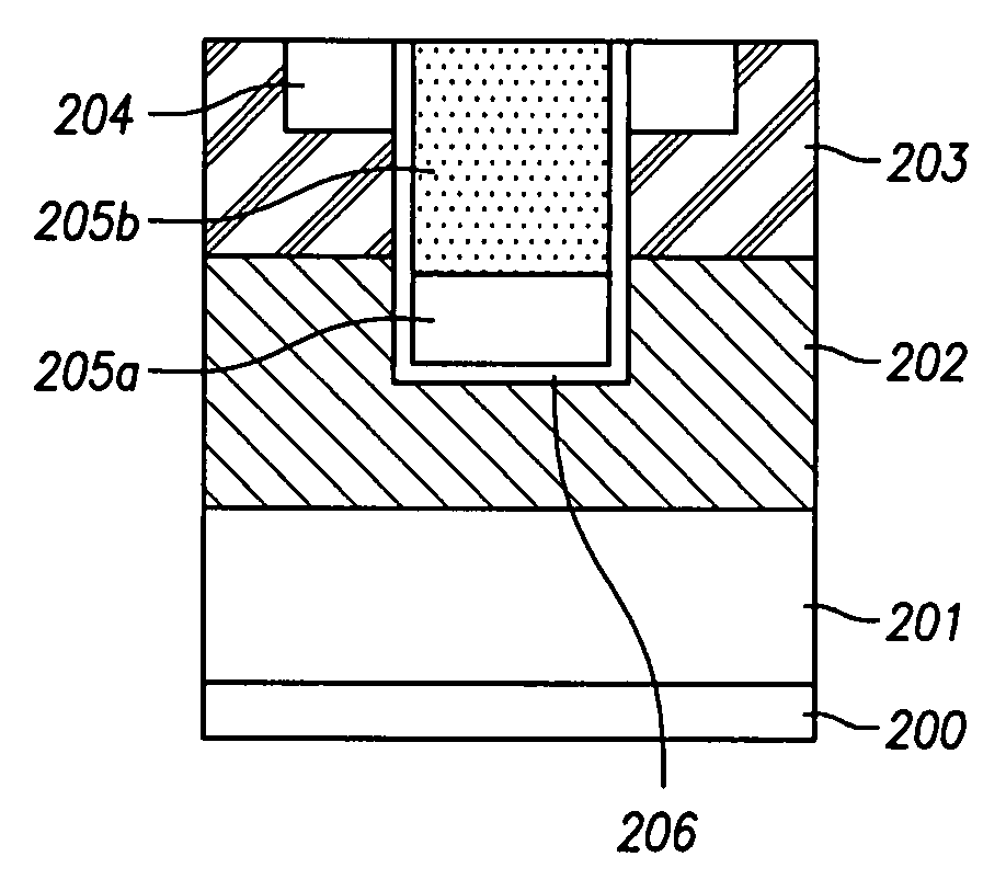
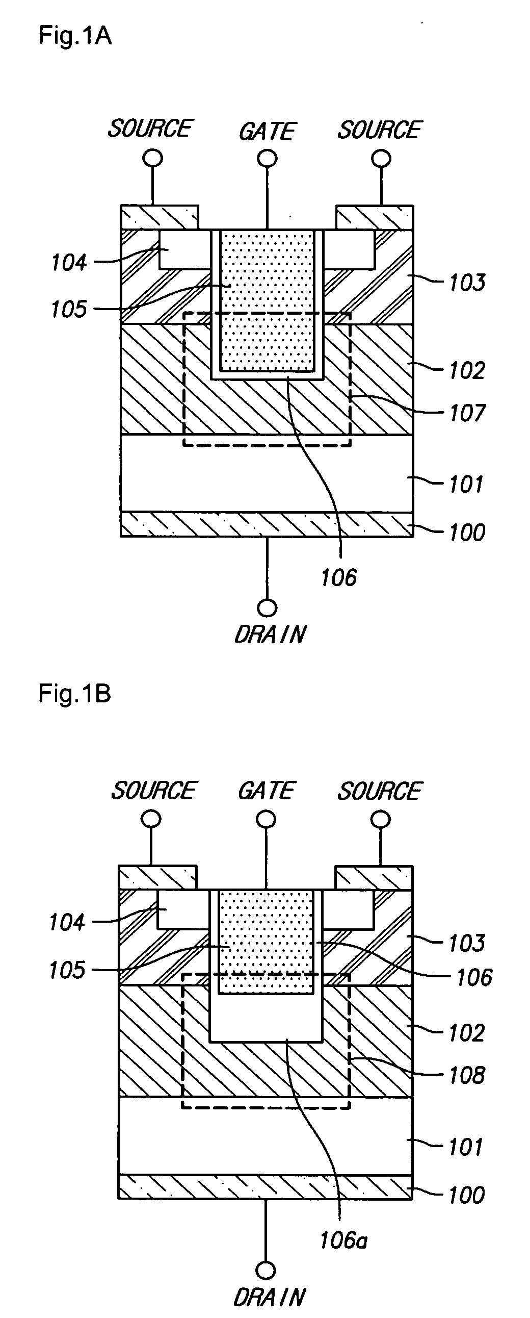
[0031]Referring to FIG. 2, the trench type MOS transistor includes a semiconductor substrate 200, a drain region 201 formed on semiconductor substrate 200, a drift region 202 formed on drain region 201, a channel body 203 formed on drift region 202, and a source region 204 formed in channel body 203. Source region 204, channel body 203, and drift region 202 may be etched to form a trench, thereby exposing a portion of drift region 202. The trench type MOS transistor further includes a gate insulating film 206 formed on inner walls of the trench, a gate electrode lower region 205a formed in a lower portion of the trench and on gate insulating film 206, and a gate electrode upper region 205b formed in the trench and on lower region 205a. In one embod...
PUM
 Abstract
Description
Claims
Application Information
 - R&D Engineer
- R&D Manager
- IP Professional
- Industry Leading Data Capabilities
- Powerful AI technology
- Patent DNA Extraction
Browse by: Latest US Patents, China's latest patents, Technical Efficacy Thesaurus, Application Domain, Technology Topic.
© 2024 PatSnap. All rights reserved.Legal|Privacy policy|Modern Slavery Act Transparency Statement|Sitemap