Method of Producing a Semiconductor Package

a manufacturing method and semiconductor technology, applied in the direction of semiconductor devices, semiconductor/solid-state device details, line/current collector details, etc., can solve the problems of reducing the resistance to improve signal transmission, and affecting the quality of semiconductor packaging

Active Publication Date: 2008-03-13
UTAC HEADQUARTERS PTE LTD
View PDF10 Cites 47 Cited by
  • Summary
  • Abstract
  • Description
  • Claims
  • Application Information

AI Technical Summary

Problems solved by technology

Advantageously, such a form of leads can shorten the transmittance distance and hence reduce resistance to improve signal transmission.
However, there are several limitations to the TAP package.
While the size of the package can be increased to maintain the die size and to accommodate the additional rows of leads,

Method used


Image

  • Method of Producing a Semiconductor Package
  • Method of Producing a Semiconductor Package
  • Method of Producing a Semiconductor Package

Examples


Embodiment Construction

[0049] Hereinafter, the present invention will be described in detail by way of exemplary embodiments with reference to the drawings. The described exemplary embodiments are intended to assist in the understanding of the invention, and are not intended to limit the scope of the invention in any way. Throughout the drawings for explaining the exemplary embodiments, those components having identical functions carry the same reference numerals for which duplicate explanations will be omitted.

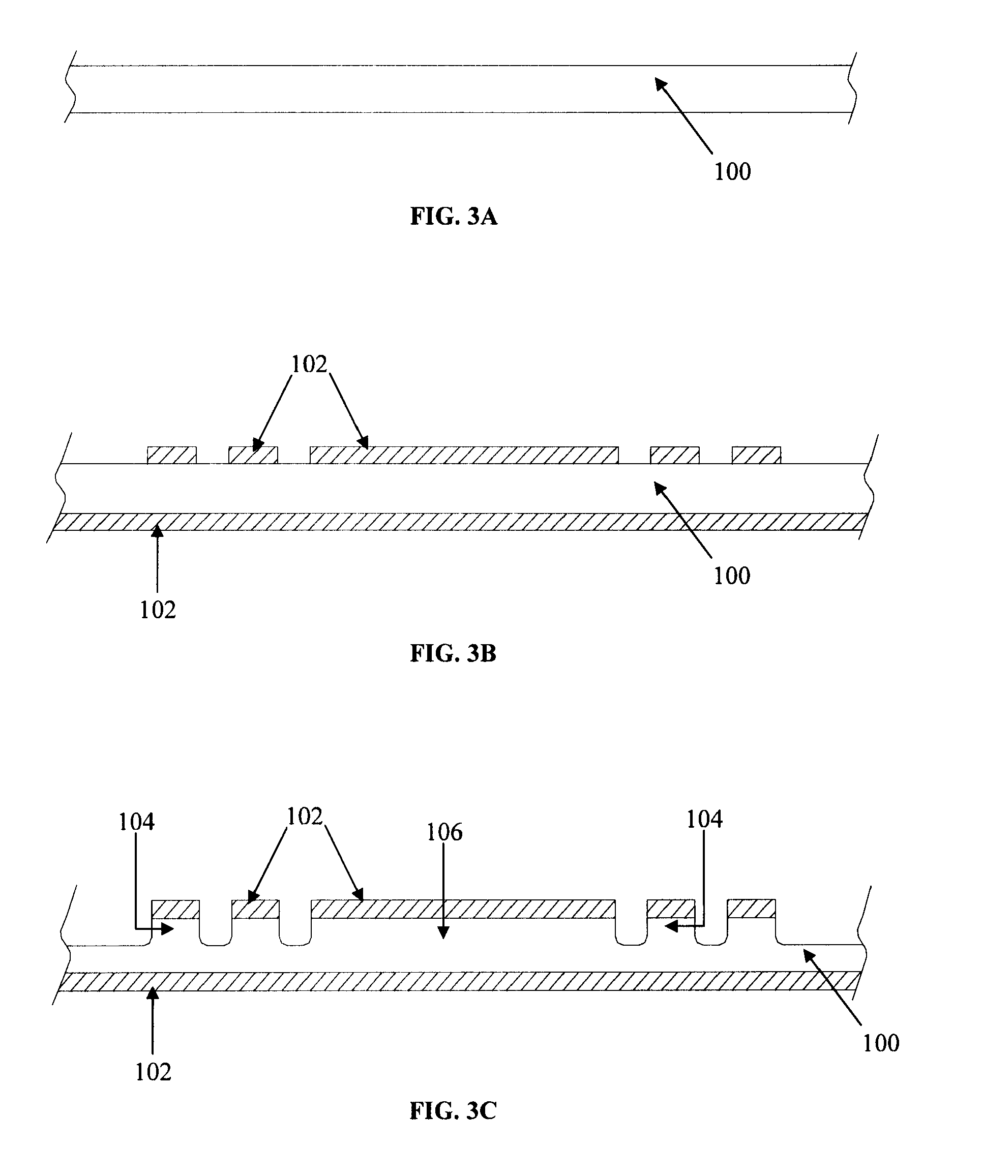
[0050] A non-limiting embodiment of a method for fabricating a semiconductor package is described below with reference to FIGS. 3A to 3M. As shown in FIGS. 3A and 3B, a resist 102 is laminated on both the top and bottom sides of a base copper layer 100. The resist 102 is developed to create a mask where terminals / leads 104 and a die pad 106 as shown in FIG. 3C can be formed in a subsequent etching process.

[0051] In FIG. 3C, the base copper layer 100 is half-etched to form terminals / leads 104 and ...


PUM

PropertyMeasurementUnit
Electrical conductivityaaaaaaaaaa
Electrical conductoraaaaaaaaaa

Abstract

A method of manufacturing a lead frame includes providing an electrically conductive layer having a plurality of holes at a top surface. The plurality of holes form a structure of leads and a die pad on the electrically conductive layer. The plurality of holes are filled with a non-conductive material. Next; an electrically conductive foil is attached on the top surface of the electrically conductive layer and the non-conductive epoxy material. Then, the electrically conductive foil is etched to create a network of leads, die pad, bus lines, dam bars and tie lines, wherein the bus lines connect the leads to the dam bar, the dam bar is connected to the tie line and the tie line is connected to the die pad.

Description

BACKGROUND OF THE INVENTION [0001] This application claims benefit of co-pending U.S. Provisional Application Nos. 60 / 840,951 and 60 / 840,954, both filed on Aug. 30, 2006, which are incorporated herein by reference.FIELD OF THE INVENTION [0002] The present invention relates to methods of manufacturing a semiconductor package and in particular, a multi-row quad flat non-leaded (QFN) package. DESCRIPTION OF THE RELATED ART [0003] A quad flat non-leaded (QFN) package is a semiconductor package that is generally used in surface mounted electronic circuit designs. The QFN package does not have external leads extending out of the package, and instead has integrated leads arranged along periphery of the die pad area at the bottom surface of the package body. Advantageously, such a form of leads can shorten the transmittance distance and hence reduce resistance to improve signal transmission. Multi-row QFN packages have two or more rows of leads surrounding the periphery of the die pad area....

Claims


Application Information

Patent Timeline
IPC IPC(8): H01L23/495H01L21/00H01R43/00
CPCH01L21/4832H01L2924/01006H01L24/45H01L24/48H01L2224/45139H01L2224/45144H01L2224/48091H01L2224/48247H01L2224/48465H01L2224/48599H01L2224/49171H01L2224/49433H01L2224/73265H01L2224/85439H01L2924/01005H01L2924/01027H01L2924/01028H01L2924/01029H01L2924/01047H01L2924/01078H01L2924/01079H01L2924/01082H01L2924/014H01L23/49582H01L2224/32245H01L24/49Y10T29/49121H01L2924/01076H01L2924/01033H01L2924/00014H01L2924/00H01L23/3107H01L23/49541H01L2224/48639H01L2924/181H01L2924/00012H01L2224/45015H01L2924/207H01L23/495H01L23/3157H01L23/49506H01L23/4952H01L23/49524
Inventor RETUTA, DANNYTAN, HIEN BOONSUN, ANTHONY YI SHENGCHEONG, MARY ANNIE
Owner UTAC HEADQUARTERS PTE LTD
Why Eureka
Try Eureka