Method for Manufacturing Gate of Non Volatile Memory Device

Inactive Publication Date: 2008-03-13
SAMSUNG ELECTRONICS CO LTD
View PDF8 Cites 4 Cited by
  • Summary
  • Abstract
  • Description
  • Claims
  • Application Information

AI Technical Summary

Benefits of technology

[0022]According to an aspect of the present invention, there is provided a method for manufacturing a gate of a semiconductor memory device comprising: forming a stacked material film including a plurality of insulating films and conductive films on an upper side of a semiconductor substrate; and performing an anisotropic etching process on the stacked material film including the plurality of insulating films and conductive films with one etching process using an etchant having a low etch selectivity on the insulating films and conductive films constituting the stacked material film.
[0023]According to another aspect of the pr

Problems solved by technology

Among these memory devices, the volatile memory devices, which are represented by DRAM (Dynamic Random Access Memory) or SRAM (Static Random Access Memory), are advantageous in that they have fast data input / output speeds, but are disadvantageous in that they can lose data stored therein as the supply of electric power is cut off.
In spite of the fact that a flash memory can store data continuously even when the supply of electric power is cut off, however, its operation speed is slower than a volatile memory.
In particular, the NOR-type flash memory device has a structure in which plural memory cells composed of single transistors are connected in parallel with each other on a bit line and a memory cell transistor is connected between a drain connected to the bit line and a source connected to a common source line, and is capable of performing a high-speed operation while increasing currents of memory cells but has difficulty in high integration due to the increase of areas occupied by bit line contacts and source line.
Undercuts created on an interface between two adjoining films (i.e. between the control floating gate 18-1 and gate interlayer dielectric film 16-1, between the gate interlayer dielectric film 16-1 and floating gate 14-1, and between the floating gate and tunnel oxide film 12-1), may cause the size of the gate pattern to be uneven and cells to be increasingly scattered from one another, which in tarn can degrade productivity and reliability of the whole semiconductor memory devices.

Method used


Image

  • Method for Manufacturing Gate of Non Volatile Memory Device
  • Method for Manufacturing Gate of Non Volatile Memory Device
  • Method for Manufacturing Gate of Non Volatile Memory Device

Examples


Embodiment Construction

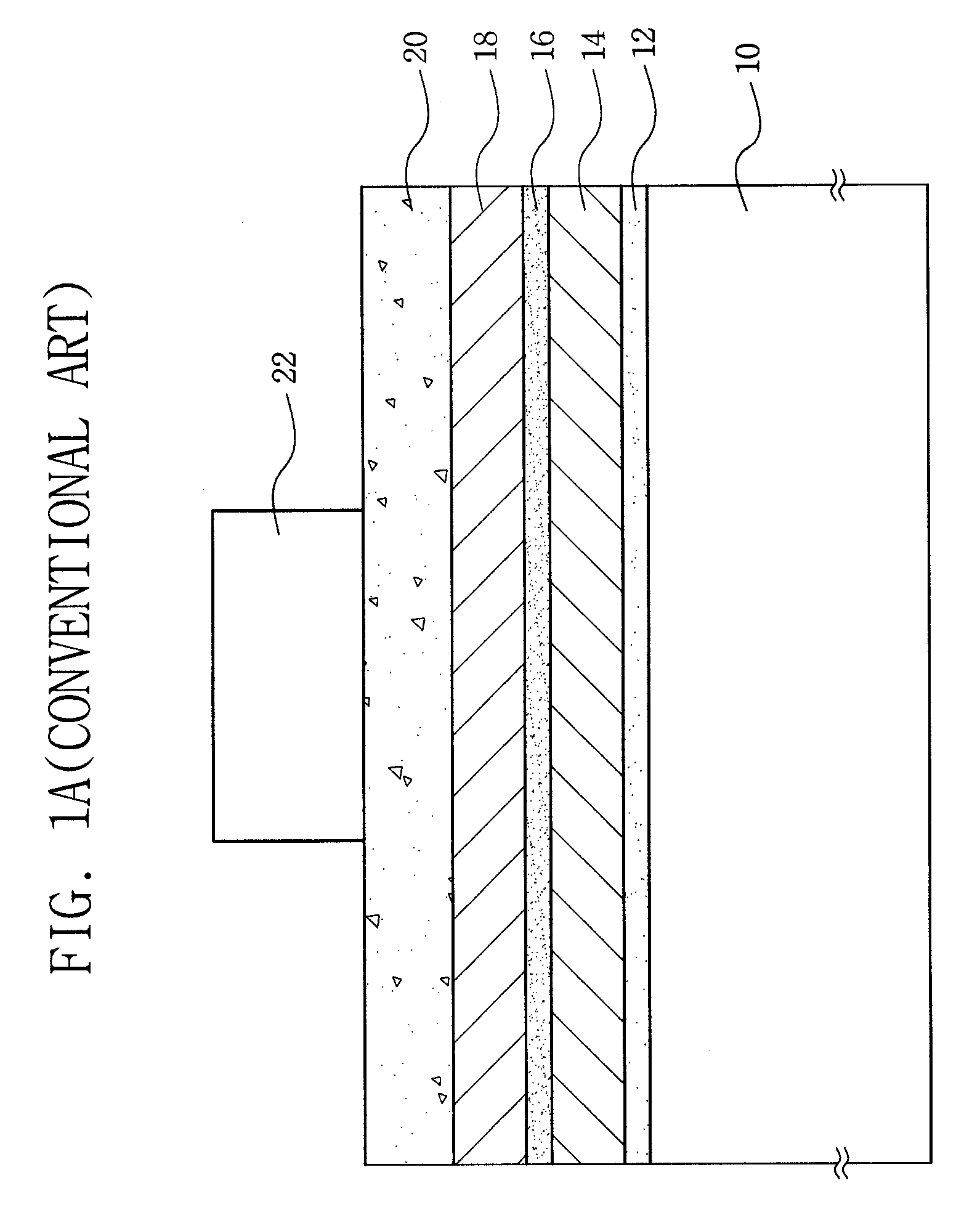
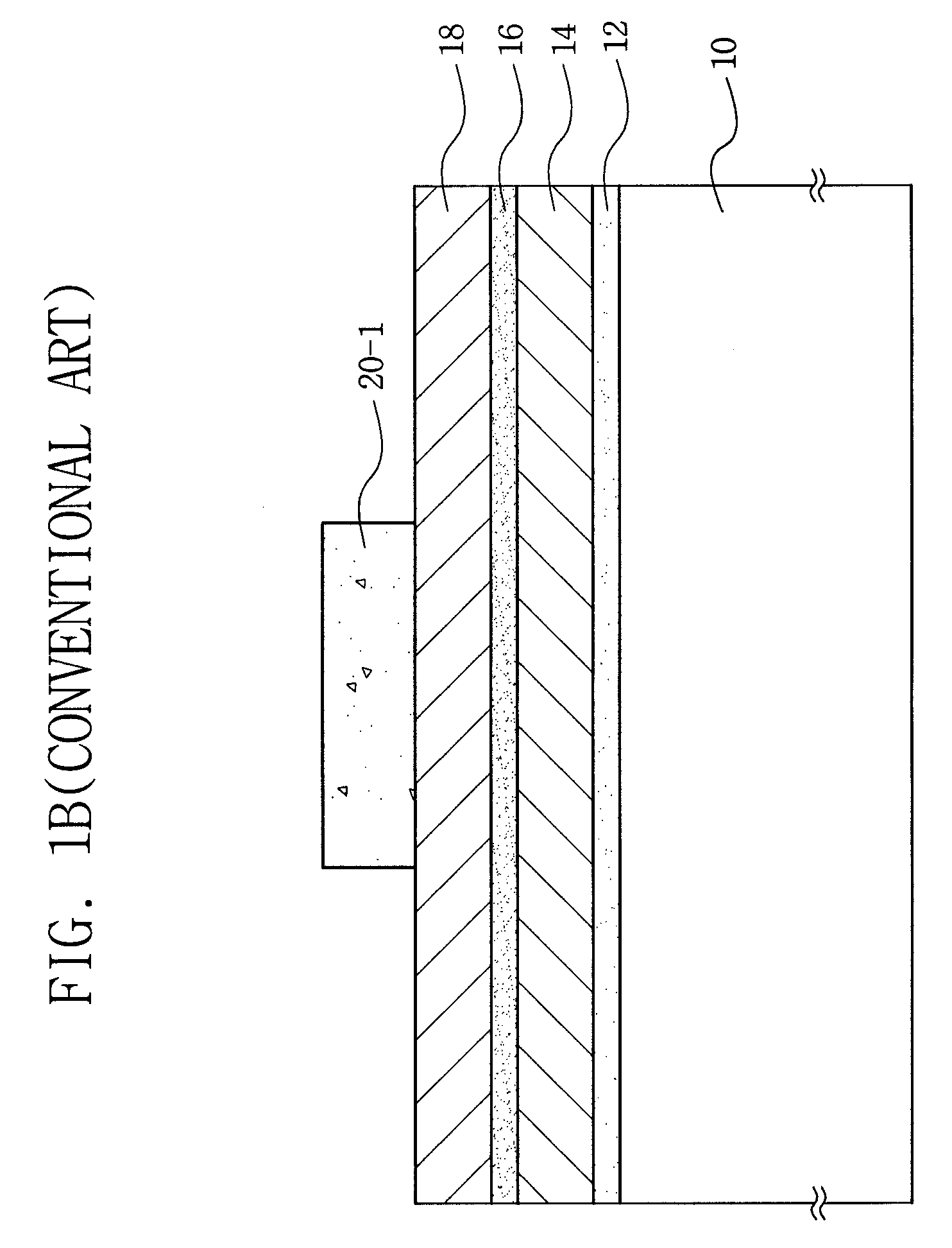
[0032]Hereinafter, exemplary embodiments of the present invention will be described in detail with reference to the accompanying drawings. However, the present invention is not limited to the embodiments disclosed hereinafter, but can be implemented in diverse forms. In the entire description of the present invention, the same drawing reference numerals are used for the same elements across various figures.

[0033]FIGS. 2a to 2c show a process forming a gate applicable to a NOR type or HAND type flash memory device according to an embodiment of the present invention.

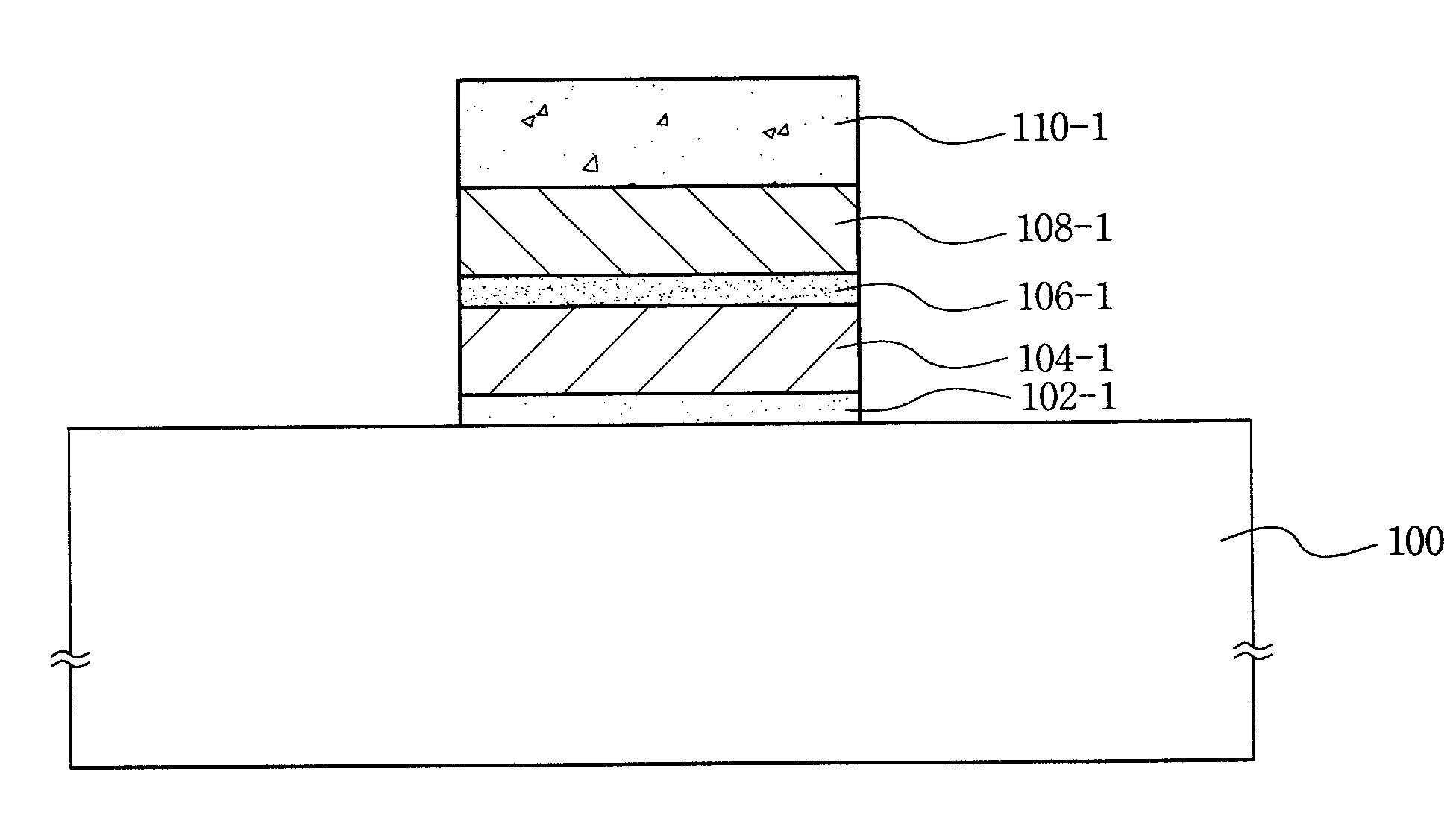
[0034]First, FIG. 2a illustrates a cross sectional view of a semiconductor substrate on which a plurality of layers are deposited to form a gate of a flash memory device.

[0035]Referring to FIG. 2a, a device separation film (not shown) is formed by carrying out a typical SIX (Shallow Trench Isolation) process on a semiconductor substrate 100 doped with N-type or P-type impurities. Subsequently, on the upper side of the semi...


PUM


Abstract

A method for manufacturing the gate of the non-volatile memory device is characterized in in-situ etching a tungsten silicide film, polycrystalline silicon films, an ONO film, and a silicon oxide film with one step using one etchant having a lower etch selectivity on the silicon and oxide films in order to form the gate. As such, in-situ etching the material films for forming the gate with one step using an etchant having a low etch selectivity on the silicon and oxide films can prevent undercuts from occurring on an interface between two different material films to thereby improve cell distribution, minimize the occurrence of particles, and reduce processing time over a prior art.

Description

CROSS-REFERENCE TO RELATED FOREIGN APPLICATIONS[0001]The present application claims priority from Korean Patent Application. No. 10-2006-0082386, filed in Korea on Aug. 29, 2006, the entire contents of which are herein incorporated by reference.BACKGROUND[0002]1. Field of the Invention[0003]The present disclosure is directed to a method for manufacturing a non-volatile memory device, and more specifically, to a method for manufacturing a gate of a non-volatile memory device.[0004]2. Description of the Background Art[0005]Semiconductor memory devices used for storing data can foe classified into volatile memory devices and non-volatile memory devices. Among these memory devices, the volatile memory devices, which are represented by DRAM (Dynamic Random Access Memory) or SRAM (Static Random Access Memory), are advantageous in that they have fast data input / output speeds, but are disadvantageous in that they can lose data stored therein as the supply of electric power is cut off. On th...

Claims


Application Information

Patent Timeline
IPC IPC(8): H01L21/3205
CPCH01L21/28273H01L21/31116H01L29/7885H01L29/7883H01L21/32137H01L29/40114H01L29/42324
Inventor KIM, YOUNG-JU
Owner SAMSUNG ELECTRONICS CO LTD
Why Eureka
Try Eureka