

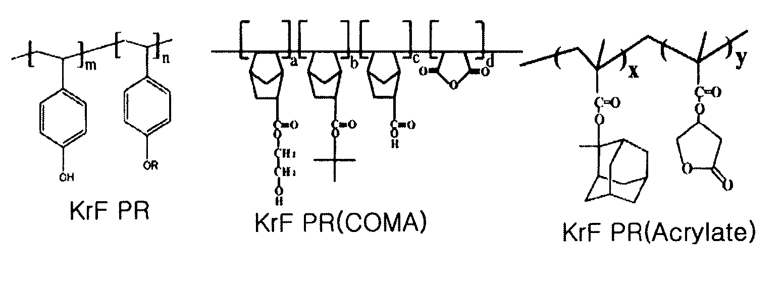
Method for fabricating semiconductor device
a semiconductor and device technology, applied in the field of semiconductor device fabrication, can solve the problems of difficult control of the process itself, cd variation due to a standing wave, and overdevelopment by reflection light due to a difference in substrate phase, etc., to achieve low etching selectivity, prevent pattern deformation, and reduce the loss of oxide-based or nitride-based hard masks
- Summary
- Abstract
- Description
- Claims
- Application Information
AI Technical Summary
Benefits of technology
Problems solved by technology
Method used
Image

Examples
Embodiment Construction
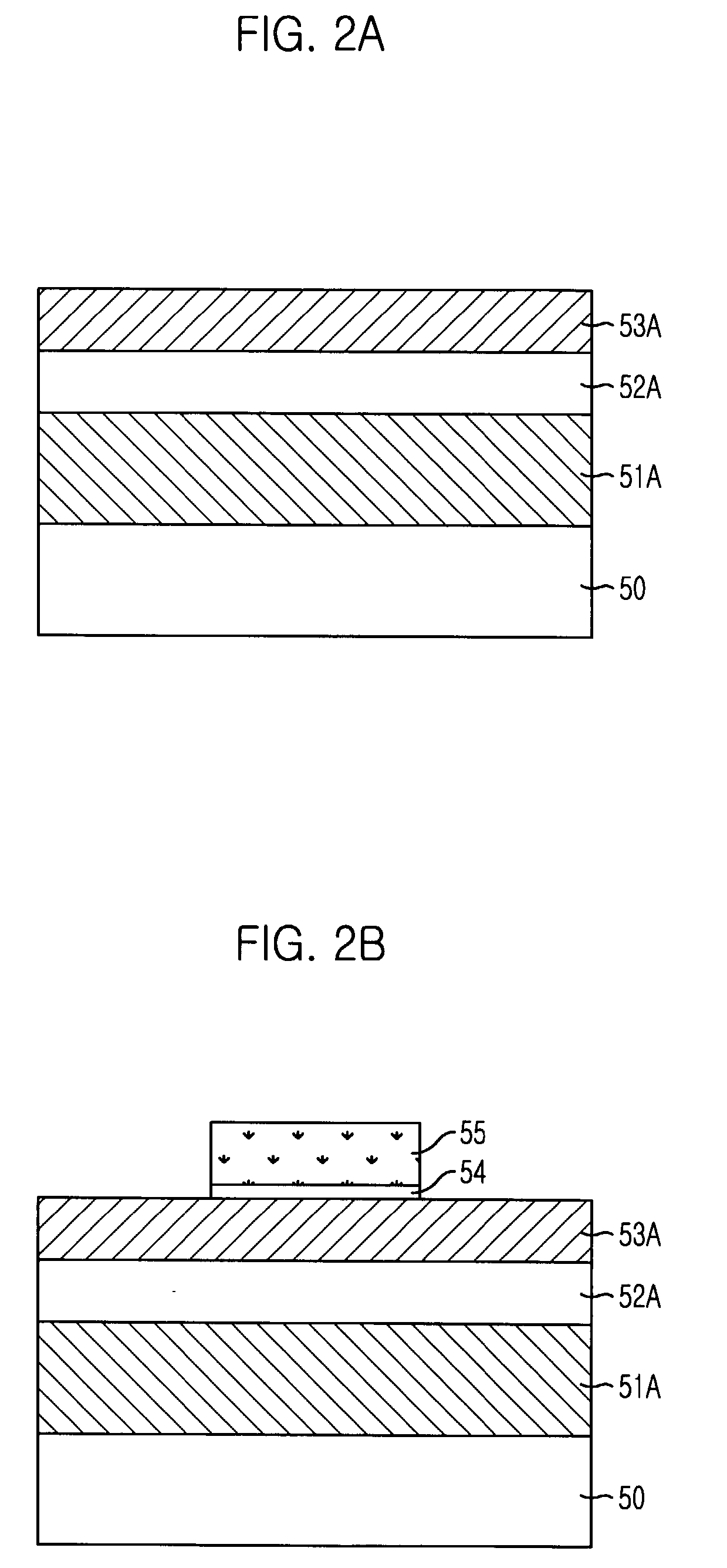
[0027] FIGS. 2A to 2D are cross-sectional views illustrating a process for forming a pattern in a semiconductor device with use of F.sub.2 or ArF light source in accordance with a first preferred embodiment. The pattern formation process will be described in more detail.
[0028] A process for forming a line pattern of a semiconductor device, more particularly, a gate electrode pattern, e.g., a word line, while patterning a conductive layer will now be disclosed. The line pattern, i.e., a conductive pattern to which the disclosed methods are applied is not limited to solely the gate electrode pattern as illustrated in the first preferred embodiment. Indeed, the line pattern is applicable for various types of the pattern formation process such as a bit line, a storage node, a metal line and so forth.
[0029] Also, in addition to the line type pattern, the disclosed methods are applicable for an isolated island type and a donut type just as a storage node contact. Instead of applying the p...
PUM
| Property | Measurement | Unit |
|---|---|---|
| wavelength | aaaaa | aaaaa |
| wavelength | aaaaa | aaaaa |
| wavelength | aaaaa | aaaaa |
Abstract
Description
Claims
Application Information