Semiconductor device and method of fabricating the same

a technology of semiconductor devices and semiconductors, applied in the direction of semiconductor devices, basic electric elements, electrical equipment, etc., can solve the problems of affecting the yield rate of semiconductor devices and the collapse of the structure, and achieve the effect of reducing the number of times of etching processes and preventing pattern deformation

Active Publication Date: 2017-04-11
MACRONIX INT CO LTD
View PDF3 Cites 0 Cited by
  • Summary
  • Abstract
  • Description
  • Claims
  • Application Information

AI Technical Summary

Benefits of technology

[0006]The invention provides a fabricating method of a semiconductor device for reducing the number of times of etching processes and preventing pattern deformation after etching or collapse of the structure.
[0027]Based on the above, the invention includes forming the trench that has the wide portions and the narrow portions having different widths, such that in the subsequent process of disposing the charge storage layer in the trench, the charge storage layer simultaneously formed in the narrow portion as the charge storage layer is formed in the wide portion can directly serve as the insulating layer. Thus, there is no need to perform an additional process to form the insulating layer. Thereby, the number of the processes of the fabricating method is reduced to prevent pattern deformation after the etching or collapse of the structure.

Problems solved by technology

However, as the device size decreases, it becomes difficult to perform alignment and control the etching processes, or the patterns may deform after the etching, which may result in collapse of the structure and affect the yield rate of fabrication of the semiconductor devices.

Method used


Image

  • Semiconductor device and method of fabricating the same
  • Semiconductor device and method of fabricating the same
  • Semiconductor device and method of fabricating the same

Examples


Embodiment Construction

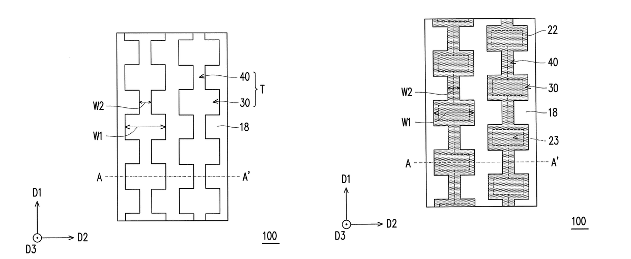
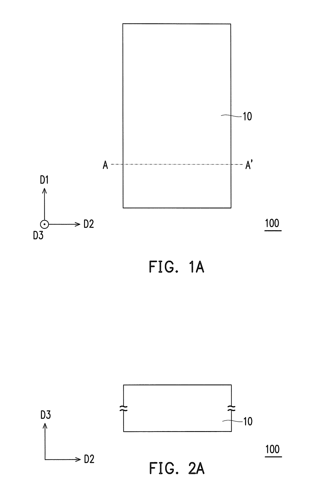
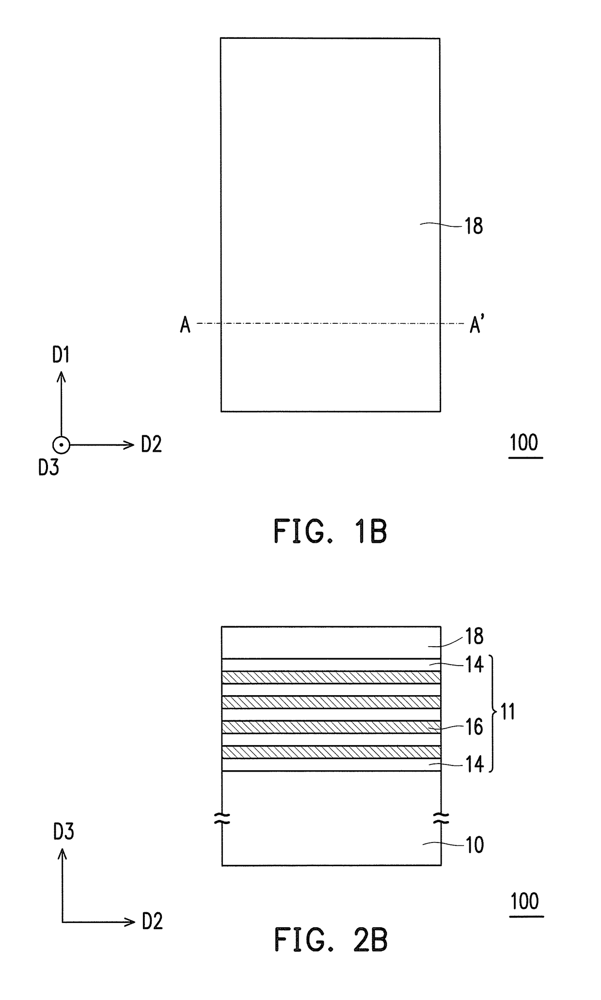
[0033]FIG. 1A to FIG. 1E are schematic top views illustrating a fabricating method of a semiconductor device according to an embodiment of the invention. FIG. 2A to FIG. 2E are schematic cross-sectional views, taken along the line A-A′ of FIG. 1A to FIG. 1E, illustrating the fabricating method of the semiconductor device.

[0034]Referring to FIG. 1A and FIG. 2A, first, a substrate 10 is provided. The substrate 10 may include a semiconductor material, an insulator material, a conductor material, or any combination of the foregoing materials. The material of the substrate 10 is a material composed of at least one selected from a group consisting of Si, Ge, SiGe, GaP, GaAs, SiC, SiGeC, InAs, and InP, or any physical structure suitable for a fabricating process of the invention, for example. The substrate 10 includes a single-layer structure or a multi-layer structure. In addition, a silicon on insulator (SOI) substrate may be used as the substrate 10. The substrate 10 is silicon or silic...


PUM


Abstract

A method of fabricating a semiconductor device is provided. A stack layer is formed on a substrate. The stack layer is patterned to form a plurality of stack structures extending in a first direction. A trench extending in the first direction is located between two adjacent stack structures. Each trench has a plurality of wide portions and a plurality of narrow portions. A maximum width of the wide portions in a second direction is larger than a maximum width of the narrow portions in the second direction. A charge storage layer is formed to cover a bottom surface and sidewalls of the wide portion and fill up the narrow portion. A conductive layer is formed to fill up the wide portion. A semiconductor device formed by the method is also provided.

Description

BACKGROUND OF THE INVENTION[0001]Field of the Invention[0002]The invention relates to a semiconductor device and a method of fabricating the same.[0003]Description of Related Art[0004]With the integration of semiconductor devices, in order to achieve high density and high performance, fabrication of semiconductor devices has evolved into stacking upward in the vertical direction, such that the wafer area can be used more efficiently. Therefore, semiconductor structures with a high aspect ratio are common in small-sized devices.[0005]When fabricating the semiconductor structures with a high aspect ratio, usually etching processes are carried out several times to form material layers having different patterns. However, as the device size decreases, it becomes difficult to perform alignment and control the etching processes, or the patterns may deform after the etching, which may result in collapse of the structure and affect the yield rate of fabrication of the semiconductor devices. ...

Claims


Application Information

Patent Timeline
Patent Type & Authority Patents(United States)
IPC IPC(8): H01L21/336H01L27/11582H01L29/792H01L21/28H01L29/10
CPCH01L27/11582H01L21/28282H01L29/1037H01L29/7926H10B43/10H10B43/27H01L29/40117
Inventor CHAN, YAO-FU
Owner MACRONIX INT CO LTD
Why Eureka
Try Eureka