

Defect imaging device and method
a technology of defect imaging and detection device, applied in the direction of instruments, nuclear engineering, and handling using diaphragm/collimeter, etc., can solve the problems of high cost and complexity of obtaining positron beams, severely limited thickness of samples under investigation by these methods, and limited application of doppler broadening spectroscopy techniques to basic materials science with little commercial or industrial application
- Summary
- Abstract
- Description
- Claims
- Application Information
AI Technical Summary
Benefits of technology
Problems solved by technology
Method used
Image

Examples
Embodiment Construction
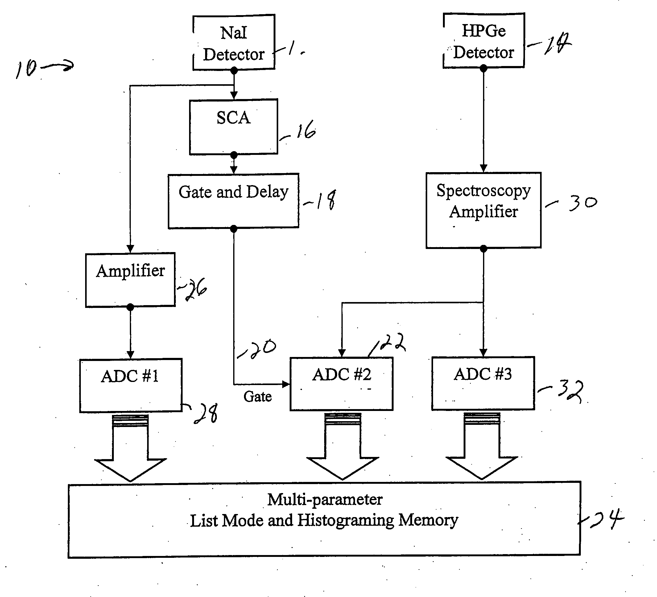
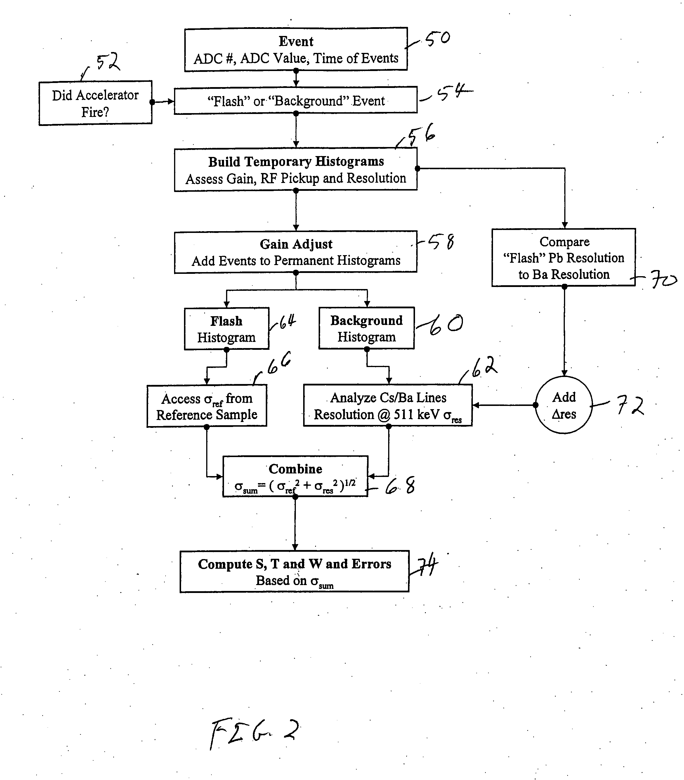
[0008]The invention enables one to analyze any material for defects deep within the material, whether a result of manufacturing defects, stress, or otherwise, and to image the defects in two and three dimensions. The invention can be applied to static or dynamic objects and materials, does not create radiation above regulatory restrictions, and is portable and highly configurable so that it can be applied in a wide variety of manufacturing environments and to virtually any object or structure, wherever it may be located. The device described herein can be used to analyze defects in objects and structures, large and small, of any construction or composition; crystal, metal, alloy, polymer, welded, bonded, cast or formed.
[0009]The invention creates positrons deep within materials with photo-nuclear methods. Three methodologies are employed to do this. The first involves the use of a bremsstrahlung beam with a maximum energy above the neutron emission thresholds to produce residual nuc...
PUM
 Abstract
Description
Claims
Application Information