Semiconductor device with a vertical MOSFET and method for manufacturing the same

a technology of vertical mosfet and semiconductor device, which is applied in the direction of semiconductor device, basic electric element, electrical apparatus, etc., can solve the problems of increased resistance value, reduced production yield, and difficult process, so as to achieve easy connection of gate wiring to refined gate connection electrode, the effect of reducing the size of the gate contact region and reducing the cos

Inactive Publication Date: 2008-03-27
NEC ELECTRONICS CORP
View PDF3 Cites 26 Cited by
  • Summary
  • Abstract
  • Description
  • Claims
  • Application Information

AI Technical Summary

Benefits of technology

[0014]According to the one embodiment of the present invention, by embedding the gate connection electrode embedded in the second trench and connecting the gate wiring to the extended part of the gate connection electrode extended from an opening of the second trench, the size of the gate contact region can be decreased without forming another conductive film different from the gate connection electrode or the gate wiring. That is, a degree of freedom can be ensured for the arrangement of via holes for making the contact with the conductive film by the gate connection electrode embedded in the second trench and extended from the opening of the second trench, in the gate contact region and the alignment margin can be ensured. Further, since the width of the via holes is enlarged, it is not necessary to form another conductive film different from the gate connection electrode and the gate wiring (for example, conductive plugs 133 shown in FIG. 7 or a connection pad in Japanese Unexamined Patent Application Publication No. HEI 7-202015 and U.S. Pat. No. 5,484,739) thereby dissolving the problem in the increase of the cost.
[0015]According to the invention, connection of the gate wiring to the refined gate connection electrode can be attained easily.

Problems solved by technology

Since the alignment margin has also to be decreased for forming such a small via hole 23, alignment at a higher accuracy is necessary, and this is difficult in view of the process and lowers the production yield as well.
Furthermore, even when the alignment can be attained with difficulty, the conductive material can not be embedded effectively if the via holes 133 are narrow to form voids or the like possibly resulting in increase in the resistance value.
However, since this method requires another conductive film as a connection pad layer, this result in a problem of increasing the production step and increasing the cost and it can not be adopted.
In the technique of forming the contact between the gate connection electrode and the gate wiring as described above, reduction of the alignment margin causes lowering of the production yield.
Further, along with refinement of the via hole size, a conductive material such as tungsten that can be formed by CVD (Chemical Vapor Deposition) and embedding into the fine via holes is necessary to result in the increase in the cost.
Furthermore, means for forming another conductive film over the trench for improving the operation efficiency of etching increases the production steps which causes increase in the cost.

Method used


Image

  • Semiconductor device with a vertical MOSFET and method for manufacturing the same
  • Semiconductor device with a vertical MOSFET and method for manufacturing the same
  • Semiconductor device with a vertical MOSFET and method for manufacturing the same

Examples


first embodiment

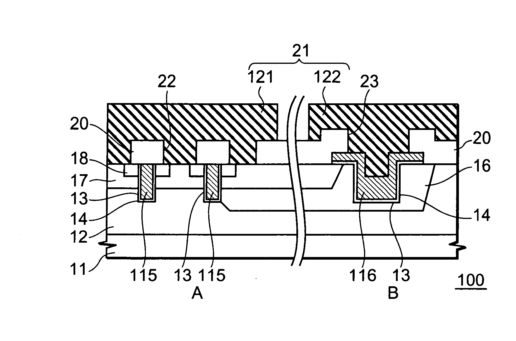
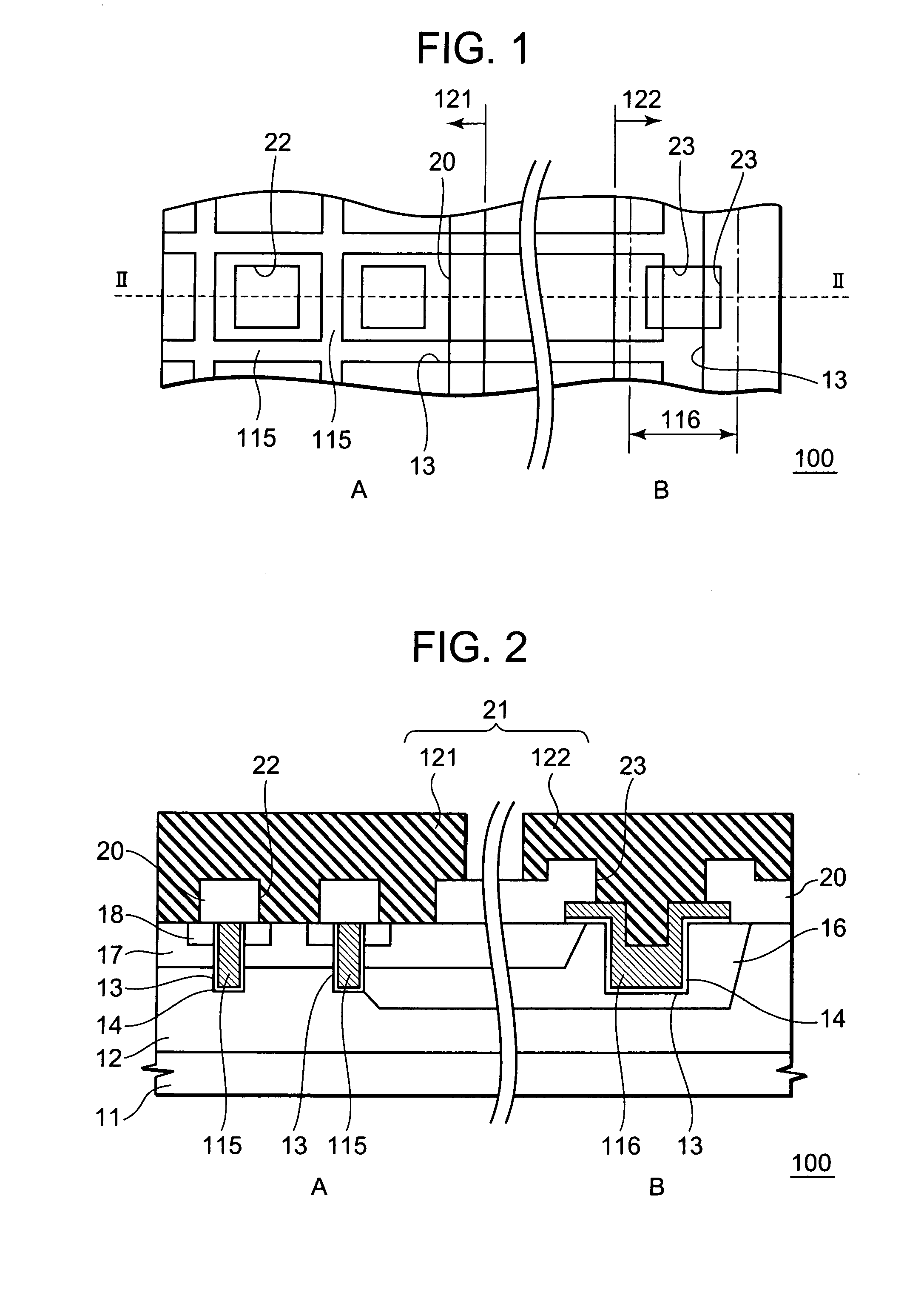
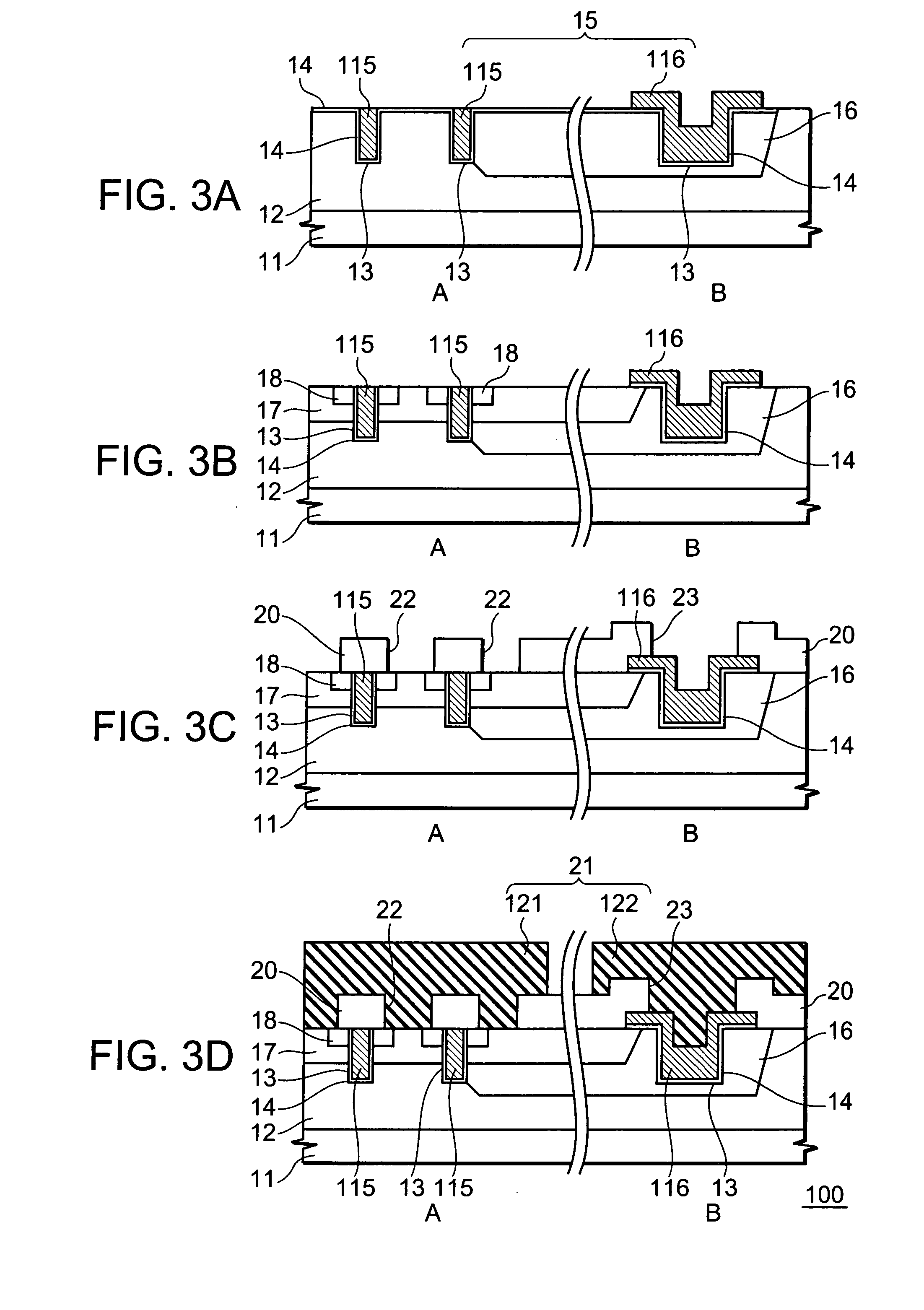
[0027]Preferred embodiments of the present invention are to be described with reference to the drawings. FIG. 1 is a fragmentary plan view of a semiconductor device 100 according to the present invention and FIG. 2 is a cross sectional view corresponding to line II-II in FIG. 1.

[0028]A semiconductor body 11 shown in FIG. 1 is an n+-type semiconductor body having an active cell region A and a gate contact region B and formed, for example, of silicon. The active cell region A means a region forming an active cell and the gate contact region B means a region in which a gate connection electrode 116 extended from a gate electrode 115 is in contact with a gate wiring 122 shown in FIG. 2. A drift region 12 is formed over the entire surface on the semiconductor body 11 by epitaxial growing. The drift region 12 is, for example, an n−-type semiconductor layer and operates together with the semiconductor body 11 as the drain of a vertical-type MOSFET. A not illustrated drain electrode is form...

second embodiment

[0047]Then, a semiconductor device 200 according to the present invention is to be described with reference to the drawings. FIG. 4 is a fragmentary plan view of the semiconductor device 200 and FIG. 5 is a cross sectional view corresponding to line V-V in FIG. 4. Since the entire constitution of the semiconductor device 200 is similar to the constitution shown in FIG. 2, therefore an explanation of the same part is to be omitted. In the semiconductor device 200, an embedded insulating film 19 is formed in the trench 13 of the gate contact region B and it is a characteristic feature that the film 19 is formed so as to cover a portion above the gate electrode 115 in the active cell region A and formed so as to cover a portion of the embedded part of the gate connection electrode 116 in the gate contact region B.

[0048]According to the semiconductor device 200, the gate electrode 115 and the source electrode 121 are electrically insulated by the embedded insulating film 19 and since it...


PUM


Abstract

The size of a gate contact region is decreased by connecting a gate connection electrode embedded in a trench and a gate wiring formed over the gate connection electrode, without forming another conductive film different from the gate connection electrode or the gate wiring. The semiconductor body includes an active cell region and a gate contact region. The active cell region includes a vertical MOSFET with a gate electrode disposed in a first trench. The gate contact region includes the gate connection electrode disposed in a second trench and formed of a same conductive material with the gate electrode. The gate connection electrode includes an embedded part formed in the second trench and an extended part extended therefrom and formed outside the second trench. An interlayer insulation film formed on the gate connection electrode and having a via hole exposing at least a portion of the embedded part of the gate connection electrode.

Description

CROSS-REFERENCE TO RELATED APPLICATIONS[0001]This application is based upon, claims the benefit of priority of, and incorporates by reference the contents of Japanese Patent Application No. 2006-260019 filed on Sep. 26, 2006.BACKGROUND[0002]1. Field of the Invention[0003]The present invention relates to a semiconductor device, and a manufacturing method thereof. More particularly, the invention relates to a semiconductor device including a vertical metal-oxide semiconductor field effect transistor (MOSFET), and a manufacturing method thereof.[0004]2. Description of Related Art[0005]Generally, vertical-type MOSFETs (metal-oxide semiconductor field effect transistor) are used for power devices such as power MOSFETs. Some power MOSFETs have a structure in which a gate electrode is formed to the inside of a trench. FIG. 7 is a cross sectional view showing the structure of a semiconductor device 10 described in Japanese Unexamined Patent Application Publication No. 2002-368221 and U.S. P...

Claims


Application Information

Patent Timeline
Patent Type & Authority Applications(United States)
IPC IPC(8): H01L29/78H01L21/336
CPCH01L29/0615H01L29/1095H01L29/4236H01L29/7813H01L29/4238H01L29/66734H01L29/7811H01L29/42376
Inventor YAMAMOTO, HIDEO
Owner NEC ELECTRONICS CORP
Why Eureka
Try Eureka