Manufacturing method and manufacturing apparatus of printed wiring board

a manufacturing method and printed wiring technology, applied in the direction of manufacturing tools, printed element electric connection formation, inspection/indentification of circuits, etc., can solve the problems of low reliability of connection between solder bump and conductor pad, and the surface of conductor pad is likely to be damaged, so as to reduce the frequency of heat history

Active Publication Date: 2008-04-03
IBIDEN CO LTD
View PDF5 Cites 21 Cited by
  • Summary
  • Abstract
  • Description
  • Claims
  • Application Information

AI Technical Summary

Benefits of technology

[0010]An object of the present invention is to provide a manufacturing method and manufacturing apparatus of a printed wiring board which enable bumps having a desired height to be formed within a requested allowable range while securing connection reliability between the solder bump and conductor pad.
[0013]According to the manufacturing method of printed wiring board of a first aspect, a low melting point metal ball is loaded on a bump having a small height or a place in which no bump is formed and then, the low melting point metal ball is melted by heating so as to intensify the height of the bump or form a bump. Thus, the heights of the bumps can be adjusted within a requested allowable range. Because when the height of the bump is intensified, a method of adding a low melting point metal ball is adopted instead of removing the bump by heating, conductor pad is not damaged thereby intensifying connection reliability between the bump and pad and further, because the printed wiring board is not subjected to local heat history, reliability of the bump of the printed wiring board can be intensified.
[0015]According to the manufacturing method of printed wiring board of a third aspect, the volume of the low bump can be obtained accurately by computing from the radius of the solder bump and a height of the solder bump from conductor pad thereby adjusting the heights of all the bumps within the allowable range.
[0022]Because according to the manufacturing method of printed wiring board of a tenth aspect, melting of the low melting point metal ball with laser is carried out with laser, the frequency of the heat history can be reduced without application of heat to the entire printed wiring board (bump having a normal height)

Problems solved by technology

However, as indicated in the JP 2003-309139 A and JP 9-64046 A, if the solder bump having a small height is melted and removed, its conductor pad surface is likely to be damaged when the solder bump is removed and when the bump is formed again, connection reliability between the solder bump and conductor pad can drop.

Method used


Image

  • Manufacturing method and manufacturing apparatus of printed wiring board
  • Manufacturing method and manufacturing apparatus of printed wiring board
  • Manufacturing method and manufacturing apparatus of printed wiring board

Examples


first embodiment

[Solder Ball Loading Apparatus]

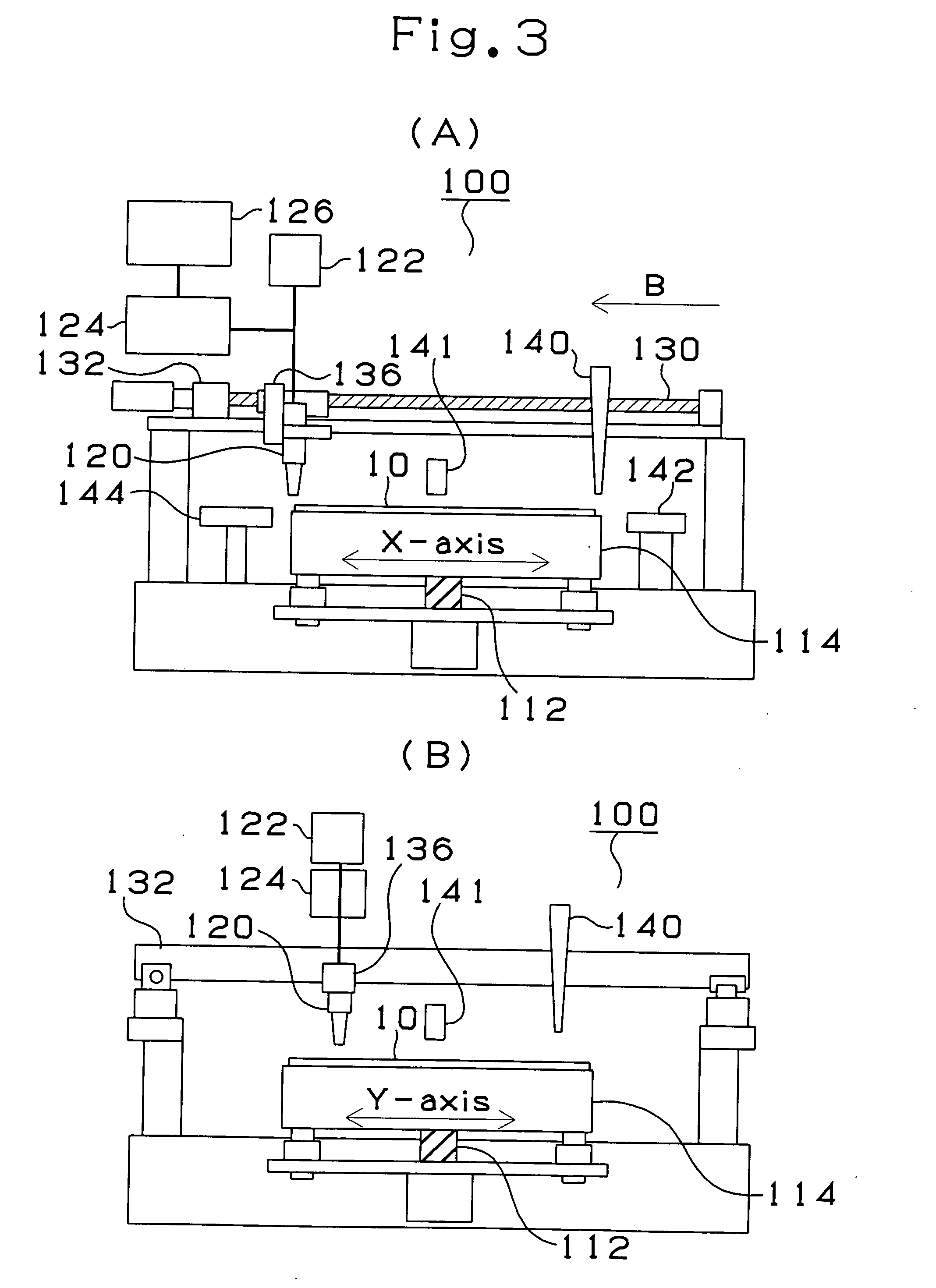
[0043]The solder ball loading apparatus for loading minute solder balls (less than 200 μm in diameter) on connection pads of a multilayer printed wiring board will be described with reference to FIG. 3. FIG. 3(A) is a structure drawing showing the structure of a solder ball loading apparatus according to the first embodiment of the present invention and FIG. 3(B) is a drawing of the solder ball loading apparatus of FIG. 3(A) as seen from the side of an arrow B.

[0044]The solder ball loading apparatus 100 comprises a Xyθ suction table 114 which positions and holds a multilayer printed wiring board 10, a vertical moving shaft 112 which lifts up and down the XYθ suction table 114, a solder ball loading cylinder 120 for introducing solder ball, a suction unit 124 for applying negative pressure and a pressure to the loading cylinder 120, a laser irradiating unit 122 which irradiates laser for melting solder balls through the loading cylinder 120, an X-direct...

second embodiment

[0059]In the first embodiment, the height of the solder bump having a small height is intensified by loading another solder bump thereon. Contrary to this, according to the second embodiment, after the volume of the solder bump is determined by measuring the height (quantity of solder) of the solder bump, a relatively large solder ball is loaded on a very low solder bump and a relatively small solder ball is loaded on a slightly low solder bump 78 so that the heights of the solder bumps fall within the narrow allowable range.

[0060]Prior to description of the second embodiment, an example of computation method of the volume of the solder bump will be described with reference to FIG. 12. The volume V when the solder bump 78S is not semi-circular but expanded flatly as shown in FIG. 12 can be obtained according to a following equation where the radius of the solder bump is r and the height thereof from the conductor pad 158P is h:

V= 4 / 3×π×r×r×h×½  [Equation 2]

[0061]In the second embodi...

third embodiment

[0065]Subsequently, the manufacturing method of printed wiring board according to the third embodiment of the present invention will be described. In the second embodiment, a solder ball corresponding to the volume of a solder ball determined by the equation 1 is selected. Contrary to this, in the third embodiment a detected amount line which indicates the relation between a bump height before correction and a bump height after correction is created preliminarily by means of experiments and simulations for each opening in a predetermined solder resist layer and a solder ball of a suitable system is selected based on this detected amount line at the time of bump correction.

[0066]This detected amount line will be described with reference to FIGS. 19, 20. FIGS. 19, 20 are graphs which indicate solder bump height before correction on its abscissa axis and solder bump height after correction on its ordinate axis. FIG. 19 shows results of tests done by correction using solder balls having...


PUM

PropertyMeasurementUnit
diameteraaaaaaaaaa
diameteraaaaaaaaaa
heightaaaaaaaaaa

Abstract

A solder ball is loaded on a bump having a small height (FIG. 5(B)) and the height of the bump is intensified by melting the solder ball by heating with laser (FIG. 5(C)). Thus, the heights of the bumps are adjusted within a requested allowable range. Because the bump is not removed by heating when the height of the low bump is intensified, the printed wiring board is not subjected to local heat history thereby intensifying reliability of the bump of a printed wiring board.

Description

BACKGROUND OF THE INVENTION[0001]1. Field of the Invention[0002]The present invention relates to a manufacturing method and manufacturing apparatus of printed wiring board and more particularly to a manufacturing method and manufacturing apparatus of printed wiring board which can be preferably used in a package board on which to mount an IC chip.[0003]2. Description of the Related Art[0004]Solder bumps are used to connect the package board and the IC chip electrically. The solder bumps are formed in following processes.[0005](1) Process for printing solder paste to a connection pad formed in an opening of solder resist layer of the package board[0006](2) Process for forming the solder bump from solder paste by reflow.[0007]After the solder bumps are formed on the package board, the IC chip is mounted on the solder bumps and by connecting the solder bumps with pads (terminals) of the IC chip by reflow, the IC chip is mounted on the package board.[0008]Currently, the quantity of sold...

Claims


Application Information

Patent Timeline
Patent Type & Authority Applications(United States)
IPC IPC(8): A47J36/02
CPCH05K1/0269H05K3/225H05K3/3478H01L2224/11334H05K2203/043H01L2924/15174H05K2203/041H01L2224/05573H01L2224/05568H01L2924/00014H01L2224/0554H01L2224/05599H01L2224/0555H01L2224/0556H05K3/40
Inventor KAWAMURA, YOICHIROTANNO, KATSUIKOIRIYAMA, MASANORIAKAI, SHO
Owner IBIDEN CO LTD
Why Eureka
Try Eureka