Solid-state imaging device

a solid-state imaging and imaging device technology, applied in the field of solid-state imaging devices, can solve the problems of increasing increasing the increasing the degree of difficulty of process associated with forming a buried insulating layer, so as to reduce the flatness of the interlayer film to be stacked on the diffusion preventing layer, the number of process steps increases, and the effect of reducing the flatness

Inactive Publication Date: 2008-04-03
PANASONIC CORP
View PDF8 Cites 35 Cited by
  • Summary
  • Abstract
  • Description
  • Claims
  • Application Information

AI Technical Summary

Benefits of technology

[0019]In view of this, it is an object of the present invention to provide a solid-state imaging device that is capable of preventing a reduction in the amount of light incident on a photodiode, has a low degree of difficulty of process, and suppresses an increase in the number of process steps.
[0040]The present invention can provide a solid-state imaging device that is capable of preventing a reduction in the amount of light incident on a photodiode, has a low degree of difficulty of process, and suppresses an increase in the number of process steps.FURTHER INFORMATION ABOUT TECHNICAL BACKGROUND TO THIS APPLICATION

Problems solved by technology

However, in the first method, such as the method shown inFIG. 2, in which layers are formed while portions of diffusion preventing layers are sequentially removed, process steps of removing portions of diffusion preventing layers are required, causing a problem that the number of process steps increases.
In the second method, such as the method shown in FIG. 3, in which after all layers are formed, portions of diffusion preventing layers above a photodiode are removed at a time and then an insulating layer is buried, the aspect ratio for burying is high and thus there is a problem that high processing techniques are required to form an buried insulating layer 722 with few defects.
In addition, when a solid-state imaging device becomes finer, the aspect ratio for burying further increases and accordingly the degree of difficulty of process associated with forming a buried insulating layer further increases.

Method used


Image

  • Solid-state imaging device
  • Solid-state imaging device
  • Solid-state imaging device

Examples


first embodiment

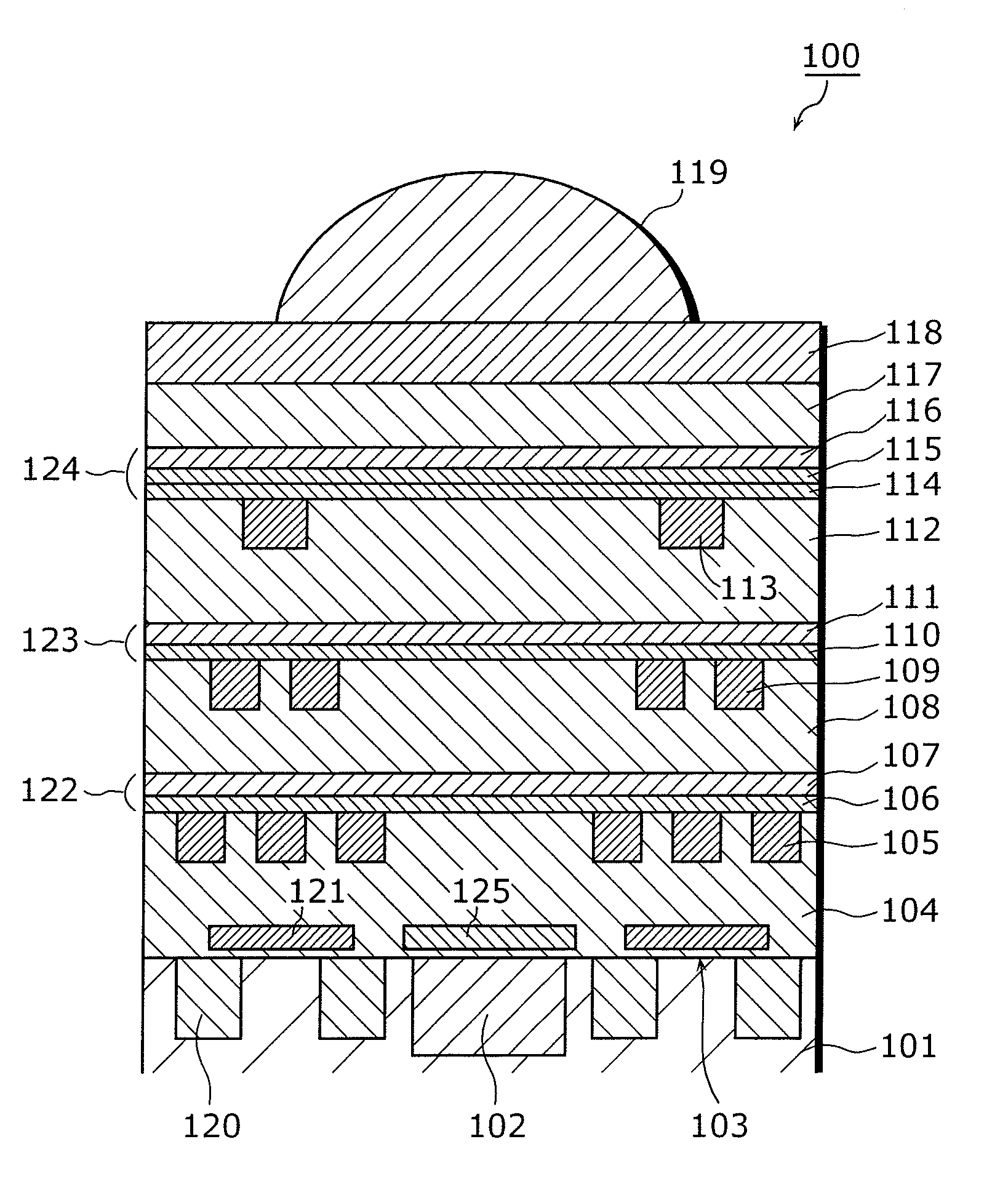
[0055]A solid-state imaging device according to a first embodiment of the present invention includes antireflection layers each having a multilayer structure and preventing reflection of incident light, as Cu diffusion preventing layers, Cu making up of Cu wirings. With this, reflection of incident light is prevented, making it possible to prevent a reduction in the amount of light incident on a photodiode.

[0056]First, a configuration of the solid-state imaging device according to the first embodiment of the present invention will be described.

[0057]FIG. 4 is a diagram schematically showing a cross-sectional structure of the solid-state imaging device according to the first embodiment of the present invention.

[0058]A solid-state imaging device 100 shown in FIG. 4 photoelectrically converts incident light and outputs an electrical signal. The solid-state imaging device 100 is a CMOS image sensor, for example. The solid-state imaging device 100 includes a semiconductor substrate 101, ...

second embodiment

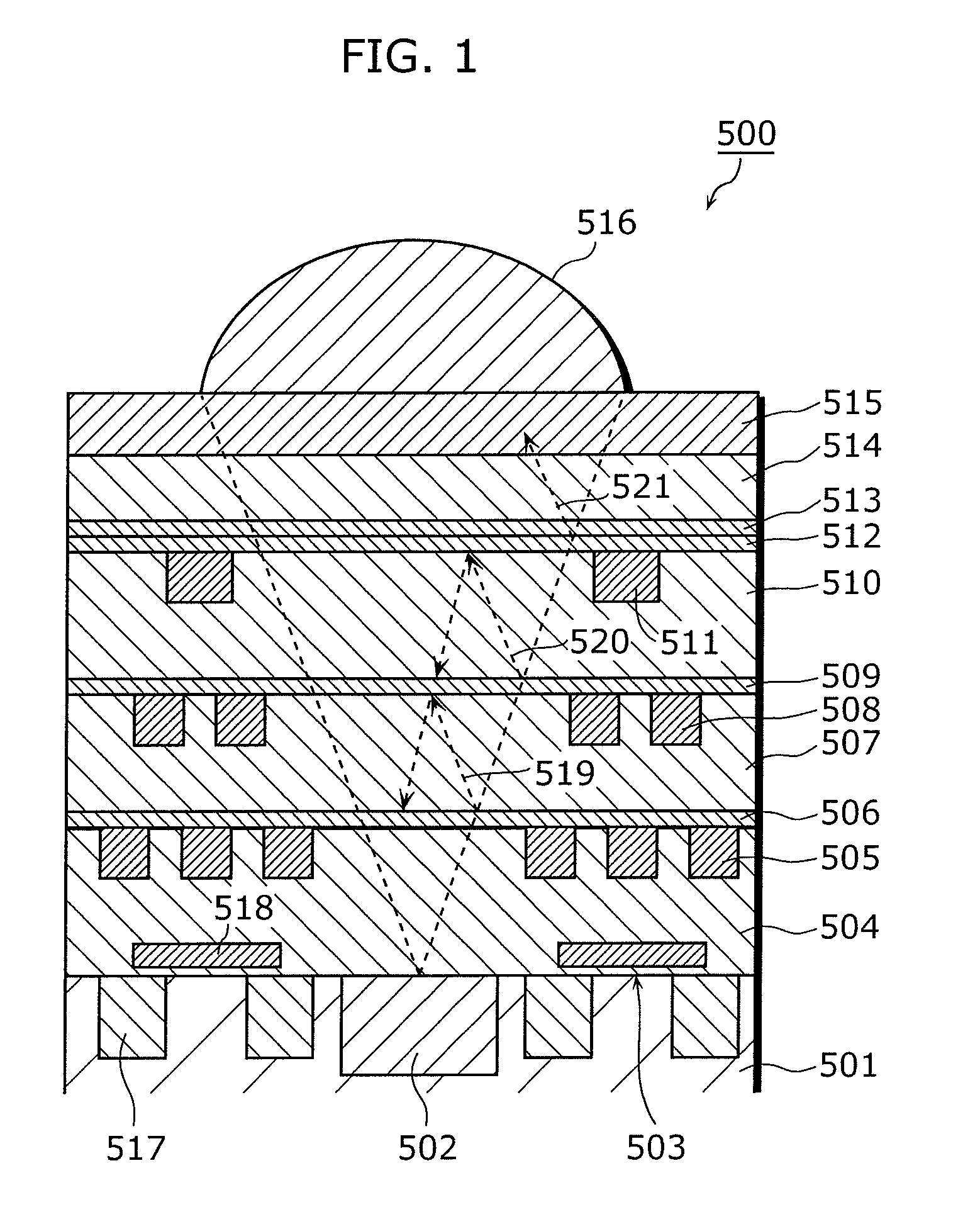
[0094]A solid-state imaging device according to a second embodiment of the present invention includes antireflection layers each having a single-layer structure and preventing reflection of incident light, as Cu diffusion preventing layers, Cu making up of Cu wirings. With this, reflection of incident light is prevented, making it possible to reduce a reduction in the amount of light incident on a photodiode.

[0095]First, a configuration of the solid-state imaging device according to the second embodiment of the present invention will be described.

[0096]FIG. 9 is a diagram schematically showing a cross-sectional structure of the solid-state imaging device according to the second embodiment of the present invention. Note that the same components as those described in FIG. 4 are denoted by the same reference numerals and a detailed description thereof will be omitted.

[0097]A solid-state imaging device 300 shown in FIG. 9 is different from the solid-state imaging device 100 according to...


PUM


Abstract

A solid-state imaging device according to the present invention includes a semiconductor substrate; a light-receiving element formed in the semiconductor substrate and photoelectrically converting incident light; and a plurality of wiring layers stacked on top of each other on a surface of the semiconductor substrate where the light-receiving element is formed. At least one of the plurality of wiring layers includes: a first insulating layer; metal wiring formed on the first insulating layer; an antireflection layer stacked on the first insulating layer and the metal wiring, preventing diffusion of a material making up of the metal wiring, and preventing reflection of the incident light; and a second insulating layer stacked on the antireflection layer.

Description

BACKGROUND OF THE INVENTION[0001](1) Field of the Invention[0002]The present invention relates to a solid-state imaging device, and more particularly to a solid-state imaging device using metal wirings having a multilayer structure and made of copper or the like.[0003](2) Description of the Related Art[0004]Solid-state imaging devices such as CMOS image sensors are used as image sensors for use in digital cameras, mobile phone cameras, web cameras, etc. In recent years, there have been an increase in the number of pixels and a reduction in the size of pixels of solid-state imaging devices. Accordingly, metal wirings to be used are changed to Cu (copper) wirings from Al (aluminum) wirings.[0005]When Cu wirings are used, since the diffusion coefficient of Cu in an oxide film is large, there is a need to form a layer that prevents Cu diffusion.[0006]FIG. 1 is a diagram showing a cross-sectional structure of a conventional solid-state imaging device using Cu wirings. A conventional soli...

Claims


Application Information

Patent Timeline
Patent Type & Authority Applications(United States)
IPC IPC(8): H01L31/0216H01L27/14H04N5/335H04N5/369H04N5/374
CPCH01L27/1462H01L27/14621H01L31/0216H01L27/14636H01L27/14627H01L27/146
Inventor MIYAGAWA, RYOHEIMAYUMI, SHUICHI
Owner PANASONIC CORP
Why Eureka
Try Eureka