Semiconductor device and method for manufacturing the same

a technology of semiconductor devices and semiconductors, applied in the direction of semiconductor devices, basic electric elements, electrical equipment, etc., can solve the problems of deterioration of the energy loss of the diode, increase of energy loss, and deterioration of the tradeoff curve of forward voltage drop (vf), so as to minimize the breakdown voltage characteristics of the p-n junction in the diode and achieve optimal carrier life. the effect of optimal carrier li

Inactive Publication Date: 2008-04-03
MITSUBISHI ELECTRIC CORP
View PDF2 Cites 20 Cited by
  • Summary
  • Abstract
  • Description
  • Claims
  • Application Information

AI Technical Summary

Benefits of technology

[0008]To solve the above-described problems, it is an object of the present invention to provide a semiconductor device wherein the variation of the breakdown voltage characteristics of the p-n junction in a diode is minimized, and can

Problems solved by technology

If the minority carriers are excessive when the diode is in the OFF state, a reverse direction current is generated to increase energy loss.
In the method using electron beam r

Method used


Image

  • Semiconductor device and method for manufacturing the same
  • Semiconductor device and method for manufacturing the same
  • Semiconductor device and method for manufacturing the same

Examples


first embodiment

[0021]A semiconductor device according to the first embodiment will be described. Here, a semiconductor device having a diode of a rated element breakdown voltage of 200 V or higher, and used in railways or the like will be described.

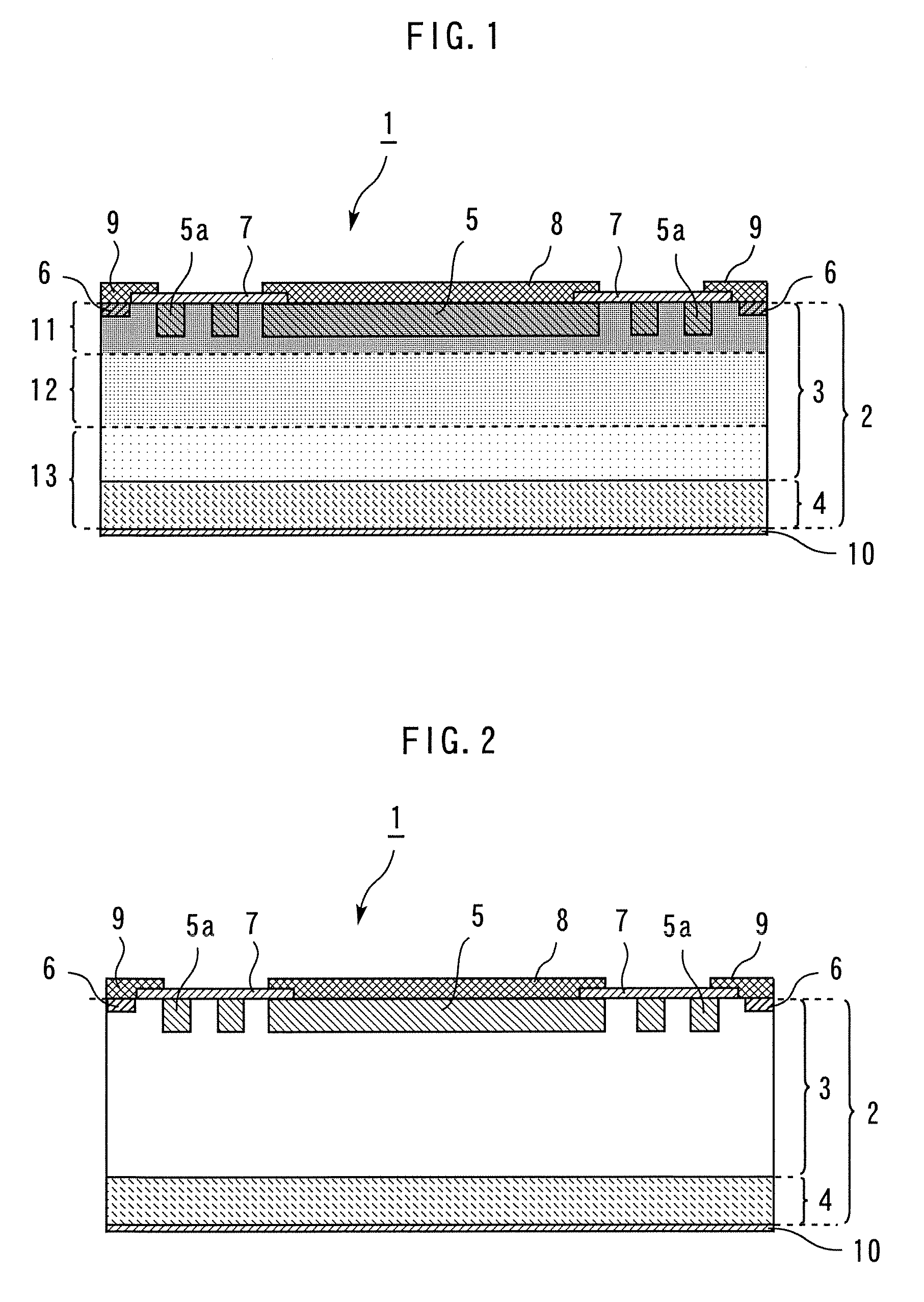
[0022]FIG. 1 shows a sectional view of the above-described semiconductor device 1. The semiconductor device 1 is formed using an n-type semiconductor substrate (hereafter simply referred to as “substrate”) 2. In the upper major surface side of the substrate 2, a low-concentration n-type impurity layer 3 containing a low-concentration n-type impurity is provided. The thickness of the layer 3 is not less than 250 μm, and the resistivity thereof is not less than 150 Ω·cm. In the lower major surface side of the substrate 2, a high-concentration n-type impurity layer 4 containing a high-concentration n-type impurity is provided so as to contact the low-concentration n-type impurity layer 3. In the vicinity of the upper major surface of the substrate 2, a p-t...

second embodiment

[0037]A method for manufacturing a semiconductor device according to the second embodiment will be described. Here, the description will be focused on the aspects different from the first embodiment.

[0038]In the same manner as in the first embodiment, a semiconductor device 1 wherein a p-n junction is provided at the interface between a p-type diffusion layer region 5 and a low-concentration n-type impurity layer 3 in the vicinity of the upper major surface of a substrate 2 (refer to FIG. 2).

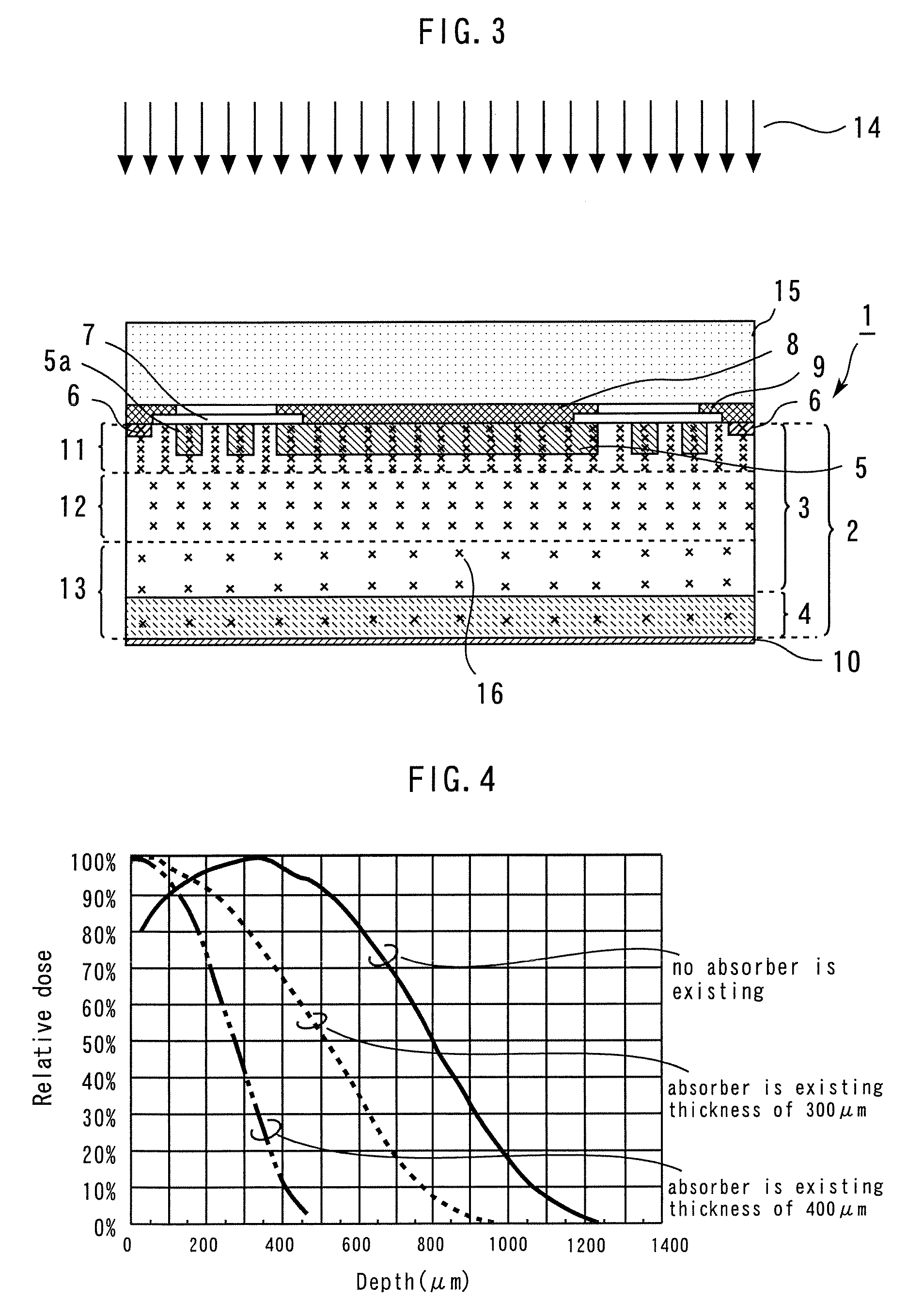
[0039]Next, as shown in FIG. 5, electron beams are radiated onto the upper major surface of the substrate 2, and crystal lattice defects 16 are formed in the substrate 2. At this time, the accelerated energy of electron-beam radiation is within a range between 400 and 500 keV. For example, electron-beam radiation of an accelerated energy of 400 keV and a dose of 3×1015 cm−2 is performed. Alternatively, electron-beam radiation of an accelerated energy of 500 keV and a dose of 1×1015 cm−2 is perfo...

third embodiment

[0049]A method for manufacturing a semiconductor device according to the third embodiment will be described. Here, the description will be focused on the aspects different from the first embodiment.

[0050]In the same manner as in the first embodiment, a semiconductor device 1 wherein a p-n junction is provided at the interface between a p-type diffusion layer region 5 and a low-concentration n-type impurity layer 3 in the vicinity of the upper major surface of a substrate 2 (refer to FIG. 2).

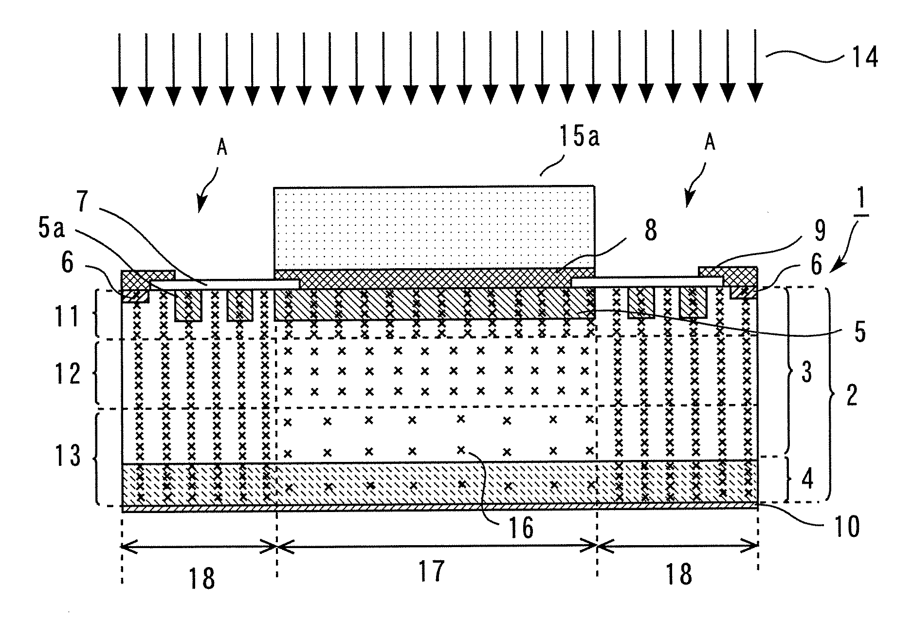
[0051]Next, as shown in FIG. 9, a mask 15a having an opening A is placed on the upper major surface of the substrate 2, and electron beams 14 are radiated through the mask 15a onto the upper major surface of the substrate 2. As the material for the mask 15a, a stainless steel having a specific gravity of 7.9 or the like is used. Thereafter, although not shown in the drawing, the semiconductor device is heat-treated in the same manner as in the first embodiment.

[0052]As a result, as shown in FIG. ...


PUM


Abstract

A p-n junction is formed at the interface of a low-concentration n-type impurity layer 3 and a p-type diffusion region 5 in the vicinity of the upper major surface of an n-type semiconductor substrate 2 of a semiconductor device 1. A mask 15 composed of an absorber is placed on the upper major surface of the semiconductor device 1, and electron beams are radiated. Thereafter, heat treatment is conducted. As a result, the peak of the crystal lattice defect densities is present in the vicinity of the upper major surface of the n-type semiconductor substrate 2, and the crystal lattice defect densities are decreasingly distributed toward the lower major surface. Thereby, a semiconductor device that can minimize the variation of the breakdown voltage characteristics of the p-n junction of the diode, and can control the optimum carrier lifetime can be obtained.

Description

BACKGROUND OF THE INVENTION[0001]1. Field of the Invention[0002]The present invention relates to a semiconductor device and a method for manufacturing the same. More specifically, the present invention relates to a semiconductor device whose characteristics and reliability are improved by introducing a carrier lifetime killer into the substrate, and a method for manufacturing the same.[0003]2. Background Art[0004]In a power semiconductor element, such as an insulated gate bipolar transistor (IGBT), a diode having a p-n junction is normally provided in the substrate. When the diode is in the ON state, minority carriers are injected through the p-n junction. If the minority carriers are excessive when the diode is in the OFF state, a reverse direction current is generated to increase energy loss.[0005]To minimize the above-described energy loss, the substrate is provided with a carrier lifetime killer, such as a crystal lattice defect. The carrier lifetime killer can recombine with th...

Claims


Application Information

Patent Timeline
IPC IPC(8): H01L29/30H01L21/263
CPCH01L21/263H01L29/861H01L29/66136H01L29/32
Inventor INOUE, MASANORI
Owner MITSUBISHI ELECTRIC CORP
Why Eureka
Try Eureka