
Semiconductor memory device with partial refresh function

a memory device and memory technology, applied in the field of semiconductor memory devices and memory systems, can solve the problems of srams consuming almost no electric power, each refresh operation ends up consuming electric current, and the operation time of batteries becomes a problem

Inactive Publication Date: 2008-04-03
SOCIONEXT INC
View PDF4 Cites 9 Cited by
  • Summary
  • Abstract
  • Description
  • Claims
  • Application Information

AI Technical Summary

Benefits of technology

[0023]According to at least one embodiment of the present invention, the frequency of the refresh timing signal is set to a sufficiently high frequency that is necessary to retain the data of all the addresses when all the refresh addresses are sequentially refreshed one by one. Regardless of whether in the case of the first operation mode in which refresh is performed intermittently by skipping the pulses of the refresh timing signal at predetermined intervals, or in the case of the second operation mode in which refresh is continuously performed with respect to consecutive addresses without refreshing other addresses, a refresh address of interest is always refreshed at constant time intervals that are determined by the frequency of the refresh timing signal. Accordingly, no matter how the area subjected to refresh is changed, a refresh operation is never delayed with respect to a given refresh address

Problems solved by technology

With such configuration, the operating time of the battery becomes a problem.
SRAM consumes almost no electric power for the purpose of data retention.
As a result, each refresh operation ends up consuming electric currents.
DRAM thus consumes some electric power even in the standby mode.
Namely, the retention of data in memory consumes electric power even when the portable equipment is not being used, thereby shortening the usable time of the battery.
This arrangement, however, gives rise to a problem as follows when a transition occurs from the ⅛ partial refresh operation (FIG.
Namely, the data of the memory cells corresponding to the word line WL0 are not refreshed within the time period necessary to retain data, so that the data may end up being lost.
This causes an increase in electric current consumption.

Method used


Image

  • Semiconductor memory device with partial refresh function
  • Semiconductor memory device with partial refresh function
  • Semiconductor memory device with partial refresh function

Examples


Embodiment Construction

[0035]In the following, embodiments of the present invention will be described with reference to the accompanying drawings.

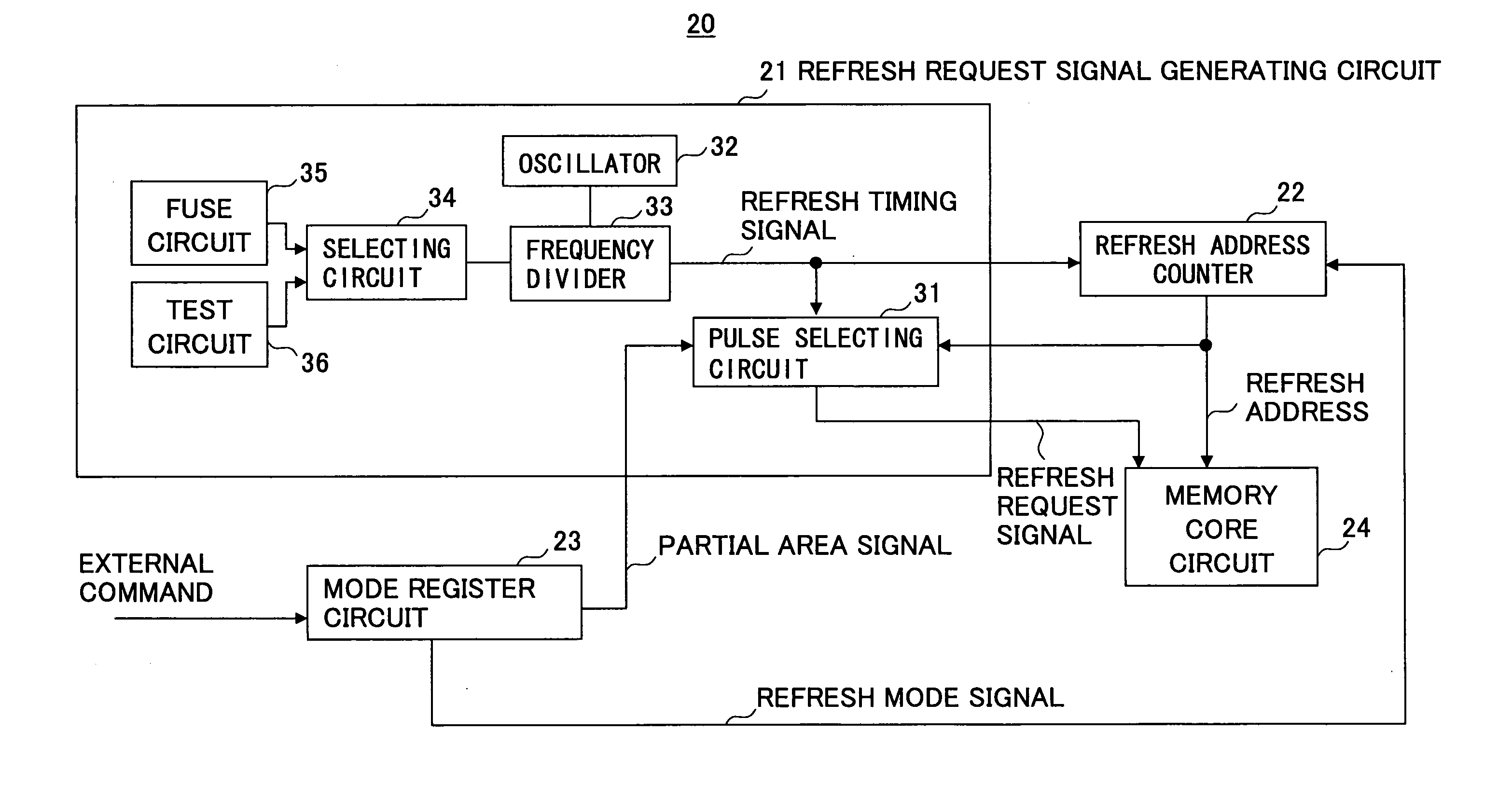
[0036]FIG. 3 is a drawing showing an example of the configuration of a semiconductor memory device according to the present invention; A semiconductor memory device 20 of FIG. 3 includes a refresh request signal generating circuit 21, a refresh address counter 22, a mode register circuit 23, and a memory core circuit 24.

[0037]The memory core circuit 24 includes a memory array, a row decoder, a column decoder, etc. The column decoder decodes a column address supplied from an external source, and activates a column selecting line specified by the column address. The row decoder decodes a row address supplied from an external source at the time of routine read / write operation, and activates a word line specified by the row address. Further, the row decoder decodes a refresh address supplied from the refresh address counter 22 at the time of refresh operation, and a...


PUM


Abstract

A semiconductor memory device includes a timing signal circuit to generate a refresh timing signal comprised of a series of pulses, a refresh address circuit to generate a refresh address in synchronization with each pulse of the refresh timing signal, a pulse selecting circuit to assert a refresh request signal in synchronization with pulses selected from the series of pulses, and a memory core to receive the refresh address and the refresh request signal and to perform a refresh operation with respect to the refresh address in response to assertion of the refresh request signal, wherein arrangement is made to switch between a first operation mode in which the selected pulses are obtained by selecting one pulse out of every predetermined number of pulses from the series of pulses and a second operation mode in which the selected pulses are obtained by selecting consecutive pulses from the series of pulses.

Description

CROSS-REFERENCE TO RELATED APPLICATIONS[0001]The present application is based upon and claims the benefit of priority from the prior Japanese Patent Application No. 2006-269629 filed on Sep. 29, 2006, with the Japanese Patent Office, the entire contents of which are incorporated herein by reference.BACKGROUND OF THE INVENTION[0002]1. Field of the Invention[0003]The present invention generally relates to semiconductor memory devices and memory systems, and particularly relates to a semiconductor memory device and memory system in which refresh can be performed with respect to part of the memory area.[0004]2. Description of the Related Art[0005]In portable terminals such as portable phones, SRAM (Static Random Access Memory) has conventionally been used. In recent years, there has been a trend to use DRAM (Dynamic Random Access Memory) for the purpose of providing a large memory capacity. With such configuration, the operating time of the battery becomes a problem.[0006]SRAM consumes ...

Claims


Application Information

Patent Timeline
IPC IPC(8): G11C7/00G11C8/00
CPCG11C5/143G11C7/1045G11C11/406G11C11/4074G11C11/40618G11C11/40622G11C11/40615G11C11/4076G11C11/401
Inventor TOMITA, HIROYOSHI
Owner SOCIONEXT INC
Learn More