
Structure and material of over-voltage protection device and manufacturing method thereof

a protection device and material technology, applied in the direction of non-metal conductors, cell components, conductors, etc., can solve the problems of high-cost semiconductor process required for manufacturing diodes, difficult control of thickness, and structure made of such a material with some defects in actual applications, etc., to achieve the effect of reducing material cost, facilitating production, and reducing manufacturing cos

Inactive Publication Date: 2008-04-03
INPAQ TECH
View PDF13 Cites 2 Cited by
  • Summary
  • Abstract
  • Description
  • Claims
  • Application Information

AI Technical Summary

Benefits of technology

[0005]Accordingly, an object of the present invention is to provide a structure and a material of an over-voltage protection device capable of reducing the manufacturing cost, and a manufacturing method thereof.
[0006]Another object of the present invention is to provide a structure and a material of an over-voltage protection device capable of simplifying the manufacturing process, and a manufacturing method thereof.
[0011]P-type and N-type semiconductor powders do not need to be purified, and they are easily obtained. Thus, the material cost is greatly reduced. Furthermore, the over-voltage protection device is not manufactured through the conventional semiconductor manufacturing process; thus, the manufacturing cost is greatly reduced as well. Moreover, since lots of pores are distributed all over the porous matrix of the over-voltage protection device in the present invention, and the k value of the air is extremely low, the over-voltage protection device of the present invention has quite a low capacitance.

Problems solved by technology

However, when abnormal charges (e.g., electrostatic charges) enter, the over-voltage protection device is changed transiently from the high impedance state to a low impedance state, and generates a transient current to conduct the abnormal invading energy to the ground end.
A high-cost semiconductor process is required when manufacturing diodes.
However, the thickness of the insulating layer according to the teaching of the above patent is less than hundreds of angstroms, so the structure made of such a material has some defects in actual applications.
For example, as the thickness of the insulating layer only falls within hundreds of angstroms, the thickness is hard to control.
When the insulting layer is too thin, a short-circuit of the device may occur; and when the insulating layer is slightly thicker, the breakdown voltage is increased.

Method used


Image

  • Structure and material of over-voltage protection device and manufacturing method thereof
  • Structure and material of over-voltage protection device and manufacturing method thereof
  • Structure and material of over-voltage protection device and manufacturing method thereof

Examples


Embodiment Construction

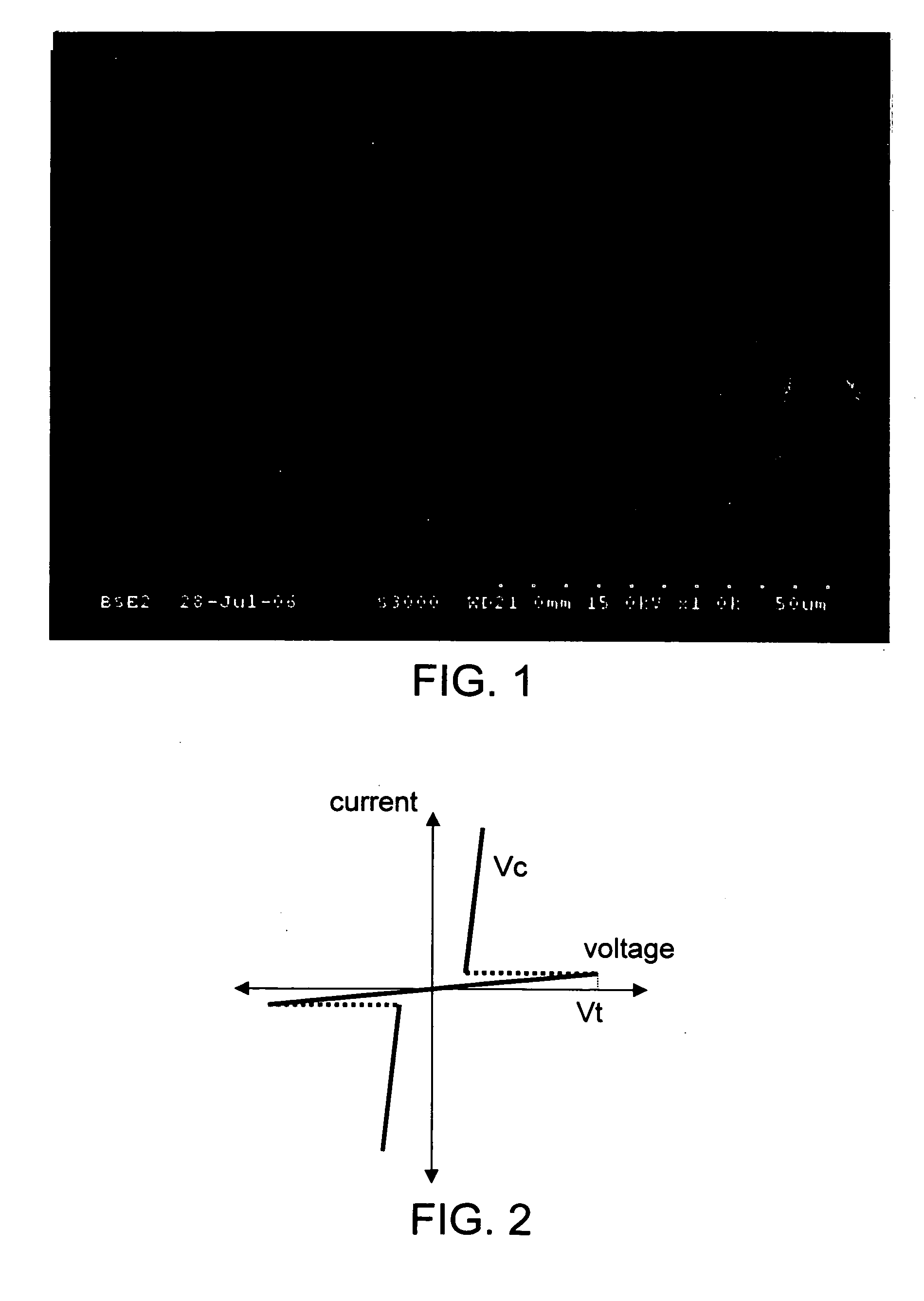
[0019]The present invention proposes a structure of a transient over-voltage protection device in an embodiment. The device includes a first electrode, a second electrode, and a porous matrix connected there between. FIG. 1 is an enlarged view of the porous matrix. In FIG. 1, the black part indicates pores. The size of the pores is approximately lower than 10 μm, and the black part takes 5%-90% of the total volume of the porous matrix.

[0020]According to an embodiment of the present invention, the material of the porous matrix includes semiconductor powder and an adhesive. Before the semiconductor powder is used to manufacture the over-voltage protection device, trivalent or pentavalent elements must be mixed into the semiconductor powder, such that the semiconductor powder has P-type or N-type characteristics. It should be noted that the present invention uses either the P-type or N-type semiconductor powders, instead of using both types of semiconductor powders. Then, a firing proc...


PUM


Abstract

The present invention relates to a material and structure of an over-voltage protection device. The material of the over-voltage protection device includes either a P-type semiconductor powder or an N-type semiconductor powder and an adhesive. The structure of the over-voltage protection device includes a first electrode, a second electrode, and a porous matrix connected between the first and second electrodes. The present invention further relates to a method of manufacturing the over-voltage protection device.

Description

FIELD OF THE INVENTION[0001]The present invention relates to a material and structure of an electronic device, and more particularly to a material and structure of an over-voltage protection device and a manufacturing method thereof.BACKGROUND OF THE INVENTION[0002]Over-voltage protection devices are widely used components in an electronic product for protecting some circuits in the electronic product from being damaged by sudden incoming charges. Generally, an over-voltage protection device is connected in parallel to both ends of the circuit to be protected, and an end of the over-voltage protection device is grounded. The over-voltage protection device is generally in a high impedance state. However, when abnormal charges (e.g., electrostatic charges) enter, the over-voltage protection device is changed transiently from the high impedance state to a low impedance state, and generates a transient current to conduct the abnormal invading energy to the ground end. Thus, the circuit ...

Claims


Application Information

Patent Timeline
IPC IPC(8): H01M8/00
CPCH01C7/1013H01C7/118H01C7/12H01L23/62H01L2924/0002H01L2924/3011H01L2924/00
Inventor LIU, TE-PANGCHANG, HSIU-YUN
Owner INPAQ TECH
Learn More