Semiconductor packaging method by using large panel size

a technology of semiconductors and panels, applied in the direction of semiconductor/solid-state device details, semiconductor devices, electrical apparatus, etc., can solve the problems of reducing the melting point of the insulating layer, etc., to achieve the effect of high melting poin

Inactive Publication Date: 2008-04-10
ADVANCED CHIP ENG TECH
View PDF15 Cites 33 Cited by
  • Summary
  • Abstract
  • Description
  • Claims
  • Application Information

AI Technical Summary

Problems solved by technology

The earlier lead frame package technology is already not suitable for the advanced semiconductor dies due to the density of the terminals thereof is too high.
However, the method is too complicated, and the molding tool 200 has a lot of spacing 204 between the package areas 202.
Another possible problem is the dice accuracy on the tape during molding process, it may cause the dice shift and twist and causing the yield loss of build-up layer and re-distribution process.

Method used


Image

  • Semiconductor packaging method by using large panel size
  • Semiconductor packaging method by using large panel size
  • Semiconductor packaging method by using large panel size

Examples


Embodiment Construction

[0015]The present invention is described with the preferred embodiments and accompanying drawings. It should be appreciated that all the embodiments are merely used for illustration. Hence, the present invention can also be applied to various embodiments other than the preferred embodiments. Besides, the present invention is not limited to any embodiment but to the appending claims and their equivalents.

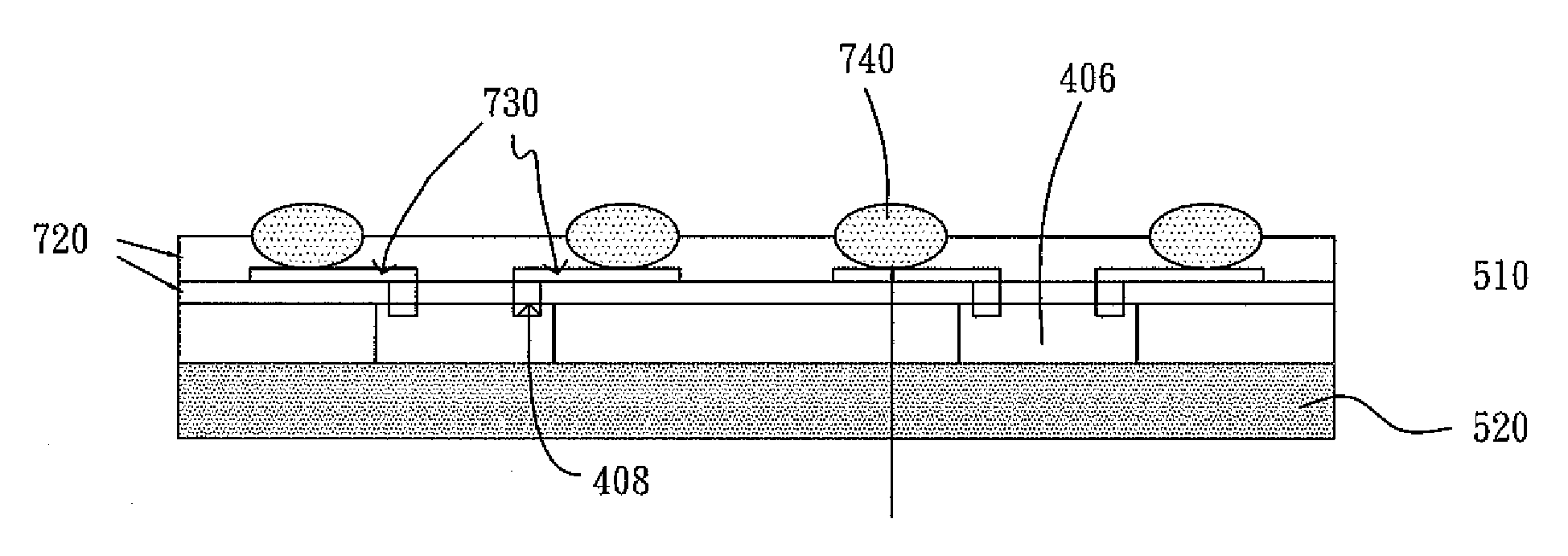
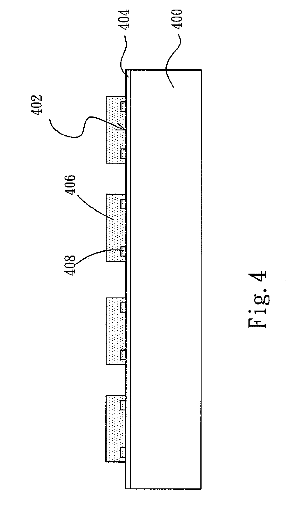
[0016]In order to achieve the present invention, a large panel size glass, such as for LCD, is prepared. Then, a back lapping process is performed to back lap the processed silicon wafer to a desired thickness, followed by dicing the processed wafer and lapped wafer into a plurality of single dice. Please refer to FIG. 4, a tool 400 for die re-distribution is prepared, the tool 400 has alignment patterns (not shown) on the top surface for the alignment during place the die. The separated dice are picked and placed on the tool 400 with the active surface 402 up site down on the tool. ...


PUM


Abstract

The present invention discloses a semiconductor packaging method, comprises steps of back lapping a processed silicon wafer to a desired thickness. Then, the dice are separated from the processed and lapped wafer into a single die. Then, the dice are picked and placed on a tool, an active surface of the dice is attached on the tool. A molding is performed to mold the dice by molding material. The tool is then removed from the dice to form a small unit. The next step is to arrange a plurality of the small units on a carrier in a matrix from. Then, a build-up layer, a re-distribution layer are formed over the dice, followed by forming solder balls on the dice. Finally, the carrier is removed.

Description

FIELD OF THE INVENTION[0001]This invention relates to a semiconductor packaging, and more particularly to a semiconductor packaging by using large panel size and lowest packaging cost per unit.BACKGROUND OF THE INVENTION[0002]The earlier lead frame package technology is already not suitable for the advanced semiconductor dies due to the density of the terminals thereof is too high. Hence, a new package technology of BGA (Ball Grid Array) has been developed to satisfy the packaging requirement for the advanced semiconductor dies. The BGA package has an advantage of that the spherical terminals has a shorter pitch than that of the lead frame package, and the terminals of the BGA are unlikely to be damage and deform. In addition, the shorter signal transmitting distance benefits to raise the operating frequency to conform to the requirement of faster efficiency. Most of the package technologies divide dice on a wafer into respective dies and then to package and test the die respectivel...

Claims


Application Information

Patent Timeline
Patent Type & Authority Applications(United States)
IPC IPC(8): H01L21/60
CPCH01L21/568H01L21/6835H01L23/5389H01L24/19H01L24/96H01L2221/68354H01L2924/01033H01L2224/20H01L2924/01075H01L2924/01077H01L2924/01078H01L2924/01082H01L2924/09701H01L2224/04105H01L2224/12105H01L2224/73267
Inventor YANG, WEN-KUNLIN, CHIH-WEIYU, CHUN-HUI
Owner ADVANCED CHIP ENG TECH
Why Eureka
Try Eureka