
OLED display device with adjusted filter array

a technology of filter array and display device, which is applied in the manufacture of electrode systems, electric discharge tube/lamps, and tube/lamp factory adjustment. it can solve the problems of reducing the overall area of the display, reducing the useable life of the lower ar device, and reducing the rejection rate of the oled display device. , to achieve the effect of reducing the overall manufacturing cost, reducing the rejection rate and high quality

Active Publication Date: 2008-04-10
GLOBAL OLED TECH
View PDF17 Cites 49 Cited by
  • Summary
  • Abstract
  • Description
  • Claims
  • Application Information

AI Technical Summary

Benefits of technology

[0012]It is therefore an object of the present invention to provide a method of making an OLED display device with an array of color filter elements that can display a high quality image even when one or more of the light producing elements are defective pixels.
[0018]The present invention provides an effect way to compensate for defective light producing elements in an OLED display device having color filter elements. A high quality image can be produced without color distortions. The presents provides a method for reducing rejected OLED display devices thereby reducing overall manufacturing cost.

Problems solved by technology

However, in this type of display device, when light is emitted downward through the substrate, the overall area that can emit light is limited by the presence of thin film transistors (TFT's) and other circuitry, which are opaque.
The result is that the lower AR devices use more power and have a shorter useable life than a device with a higher AR.
When manufacturing organic EL displays, problems such a particle contamination or scratches in the organic EL materials can result in defects in a display.
One type of defect that is caused by particle contamination or scratches is a short circuit through the thin organic materials, connecting the anode and the cathode.
Similarly, defects due to particles, scratches, mask-errors, electrostatic discharge (ESD), and similar manufacturing problems can occur in the manufacturing of the active matrix circuitry of an active matrix OLED display device which results in non-functional pixels or pixels which emit at an incorrect luminance level (dim or bright).
Alternately, defects in the active matrix circuitry can result in a condition where a pixel continuously emits during operation and can not be selectively turned off.
Many of these manufacturing defects, typically occur with an area density that depends on the capability of the manufacturing process, equipment and the environment.
In a multicolored device, a dead, dim, bright, or stuck-on pixel in one color can cause color distortions in the image.

Method used


Image

  • OLED display device with adjusted filter array
  • OLED display device with adjusted filter array
  • OLED display device with adjusted filter array

Examples


first embodiment

[0039]Turning now to FIG. 5a, an OLED display device according to the present invention is shown having an array of light producing elements 52 including a defective light producing element 210x. In this case, a short-circuit defect 170 is present connecting the anode and cathode of organic light emitting diode 150x. Short circuit defect 170 is represented by a resistor having a resistance ranging from approximately 100 Kohms to nearly 0 ohms. This short circuit defect 170 could be caused, for example, by a particle defect of a scratch defect in the organic electroluminescent media in the organic light emitting diode 150x. Short circuit defect 170 is an example defect to which the present invention could be applied. The present invention can also be applied to other types of defects, including defective transistors and opens and shorts in the transistors and the wires connecting the transistors. Defective transistors include transistors with abnormal characteristics such as threshol...

second embodiment

[0068]Turning now to FIG. 11, a cross-section of an OLED display device according to the present invention is shown. In this embodiment, the array of color filter elements, such as color filter element 220a, are formed directly over the light producing elements, such as light producing element 210a which is formed over first substrate 100. This approach of forming the color elements directly over the light producing elements eliminates the need for a second substrate, which can reduce material costs, provide a thinner final display unit, and simplify the manufacturing equipment. As in the prior embodiments, the color filter elements are still preferably deposited by a mask-less process such as ink jet printing. As in the prior embodiments, the locations of the color filter elements are adjusted using the mask-less process in response to the recorded location of any defective light producing elements as determined by testing the array of light producing elements.

[0069]In this second ...


PUM


Abstract

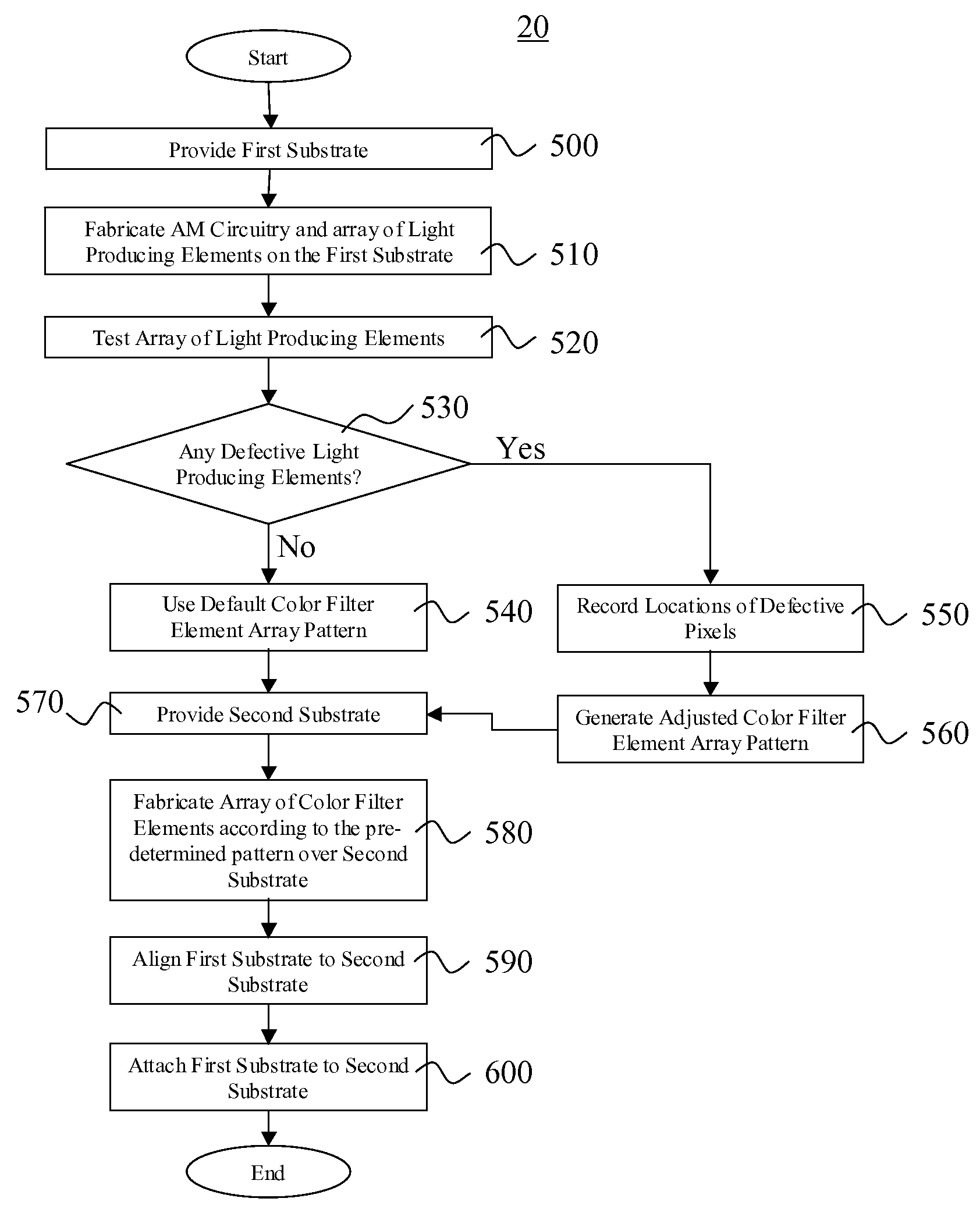
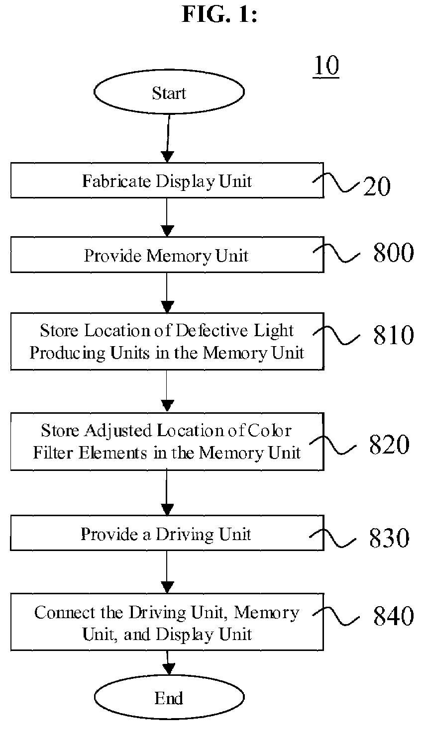
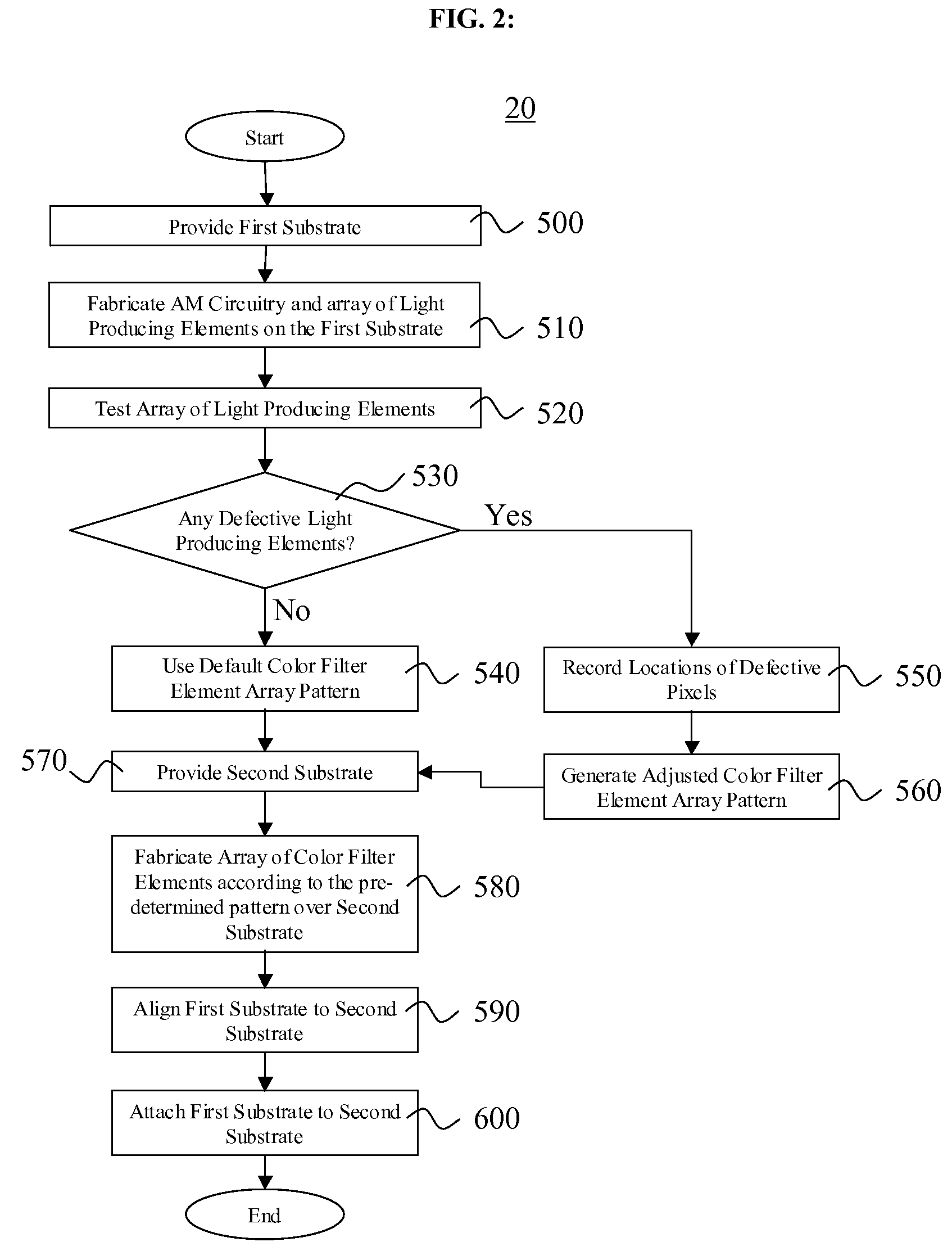
A method of making an OLED display device for producing an image includes forming an array of light producing elements; testing the array of light producing elements and recording the location of defective light producing element(s); providing a default pattern of the array of color filter elements having at least two different colors; and forming an array of color filter elements in response to the recorded location of the defective light producing element(s), the location of at least one color filter element being changed from the default pattern.

Description

CROSS REFERENCE TO RELATED APPLICATIONS[0001]Reference is made to commonly assigned U.S. patent application Ser. No. 11 / 040,066 filed Jan. 21, 2005 entitled “Method and Apparatus for Defect Correction in a Display” by Ronald S. Cok; U.S. patent application Ser. No. 11 / 274,467 filed Nov. 15, 2005 entitled “Method and Apparatus for Defect Correction in a Display” by Ronald S. Cok et al; and U.S. patent application Ser. No. 11 / 289,986 filed Nov. 30, 2005 entitled “OLED Devices with Color Filter Array Units” by Dustin L. Winters, the teachings of which are incorporated herein.FIELD OF THE INVENTION[0002]The present invention relates to making OLED display devices with an array color filter elements that is changed in response to defective light producing elements.BACKGROUND OF THE INVENTION[0003]In the simplest form, an organic electroluminescent (EL) device is comprised of an organic electroluminescent media disposed between first and second electrodes serving as an anode for hole inje...

Claims


Application Information

Patent Timeline
IPC IPC(8): H01J9/20H01J9/44
CPCH01L27/322H01L2251/568H01L2251/5315H01L51/56H10K59/38H10K2102/3026H10K71/861H10K71/70H10K71/00
Inventor WINTERS, DUSTIN L.
Owner GLOBAL OLED TECH
Learn More