Split gate non-volatile memory devices and methods of forming the same

a non-volatile memory and split-gate technology, applied in the direction of semiconductor devices, electrical devices, transistors, etc., can solve the problems of punch-through and junction breakdown due to an increase in the source depletion region, data retention and cycling endurance performance problems, etc., to achieve enhanced programming and erasing efficiency and performance, and the effect of increasing the floating gate coupling ratio

Inactive Publication Date: 2008-04-24
SAMSUNG ELECTRONICS CO LTD
View PDF6 Cites 28 Cited by
  • Summary
  • Abstract
  • Description
  • Claims
  • Application Information

AI Technical Summary

Benefits of technology

[0018] In general, exemplary embodiments of the invention include non-volatile memory devices and methods for fabricating non-volatile memory devices. More specifically, exemplary embodiments of t

Problems solved by technology

Although the conventional split-gate memory framework of FIG. 1A provides advantages over other conventional non-volatile memory designs, the split-gate framework of FIG. 1A can suffer performance problems with respect to data retention and cycling endurance.
Over time, the continuous application of such high voltage to the control gate (16) can adversely affect and stress the dielectric material of the tunneling layer (19) causing

Method used


Image

  • Split gate non-volatile memory devices and methods of forming the same
  • Split gate non-volatile memory devices and methods of forming the same
  • Split gate non-volatile memory devices and methods of forming the same

Examples


Embodiment Construction

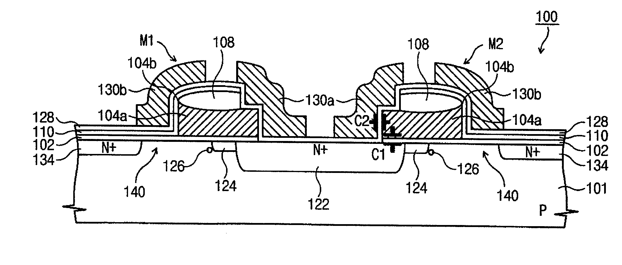
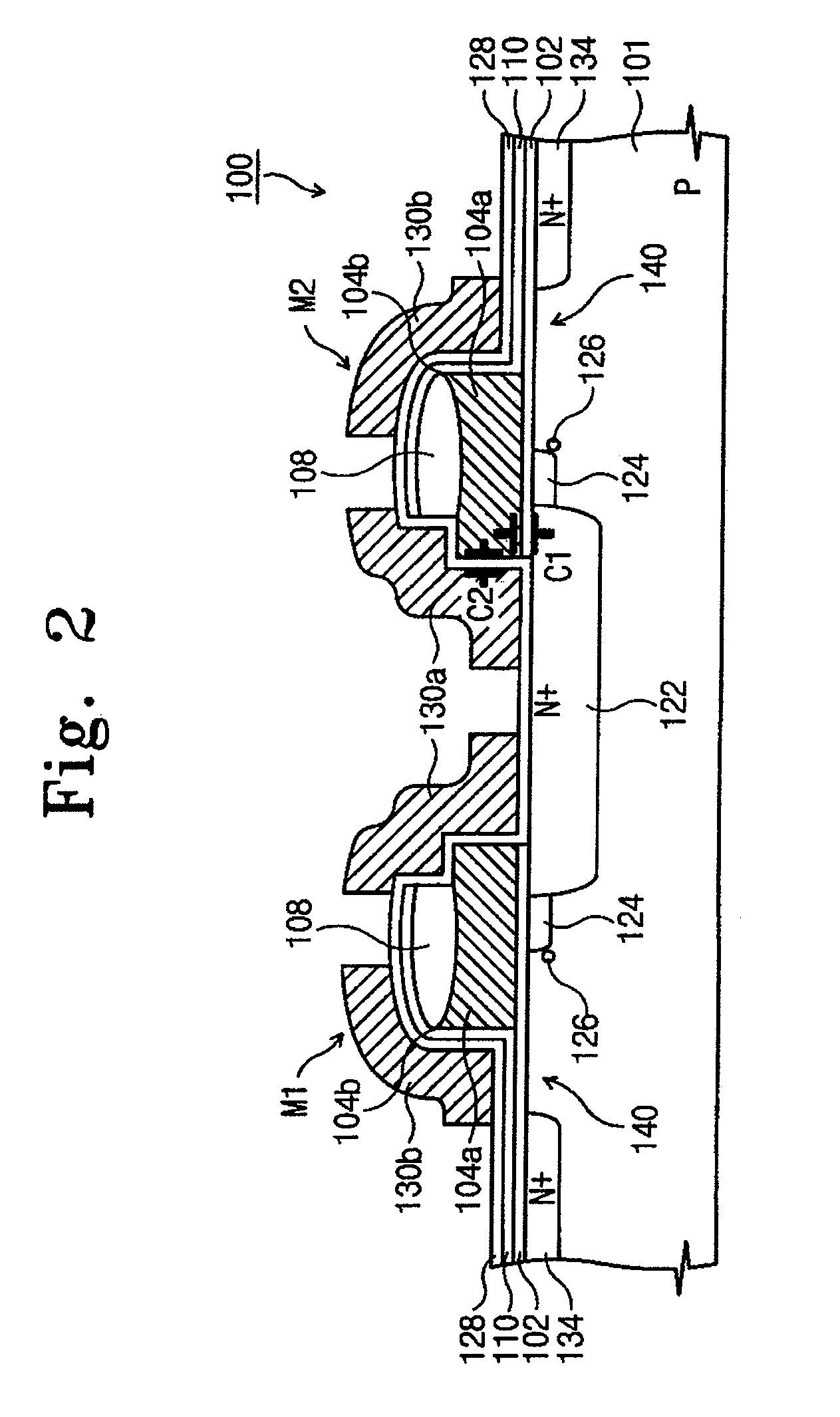
[0029] Exemplary embodiments of the invention will now be described more fully with reference to the accompanying drawings in which it is to be understood that the thickness and dimensions of the layers and regions are exaggerated for clarity. It is to be further understood that when a layer is described as being “on” or “over” another layer or substrate, such layer may be directly on the other layer or substrate, or intervening layers may also be present. Moreover, similar reference numerals used throughout the drawings denote elements having the same or similar functions.

[0030]FIG. 2 is a cross-sectional schematic view of a split gate non-volatile memory device (100) according to an exemplary embodiment of the invention. In particular, FIG. 2 depicts two split-gate memory cells M1 and M2 formed on a p-type semiconductor substrate layer (101). A plurality of diffusion regions (122) and (134) are formed in the substrate (101). In particular, in one exemplary embodiment, the diffusi...


PUM


Abstract

Non-volatile memory devices and methods for fabricating non-volatile memory devices are disclosed. More specifically, split gate memory devices are provided having frameworks that provide increased floating gate coupling ratios, thereby enabling enhanced programming and erasing efficiency and performance.

Description

CROSS-REFERENCE TO RELATED APPLICATION [0001] This application is a divisional of U.S. patent application Ser. No. 11 / 368,247, filed on Mar. 3, 2006 which claims priority under 35 U.S.C. Section 119 to Korean Patent Application No. 2005-18771, filed on Mar. 7, 2005, the disclosures of which are each incorporated herein by reference in their entirety.TECHNICAL FIELD OF THE INVENTION [0002] The present invention relates generally to non-volatile memory devices and methods for fabricating non-volatile memory devices. More specifically, the present invention relates to split gate memory devices having frameworks that provide increased floating gate coupling ratios, thereby enabling enhanced programming and erasing efficiency and performance. BACKGROUND [0003] In general, non-volatile memory devices are memory devices that will retain stored data even while power is off. Typically, non-volatile memory devices are utilized in various products and devices, such as mobile telecommunication ...

Claims


Application Information

Patent Timeline
IPC IPC(8): H01L29/788
CPCH01L29/7887H01L29/66825
Inventor KANG, SUNG-TAEGKWON, HYOK-KISEO, BO YOUNGYOON, SEUNG BEOMJEON, HEE SEOGCHOI, YONG-SUKHAN, JEONG-UK
Owner SAMSUNG ELECTRONICS CO LTD
Why Eureka
Try Eureka