Light emitting diode and wafer level package method, wafer level bonding method thereof, and circuit structure for wafer level package

a technology wafers, applied in the direction of basic electric elements, electrical apparatus, semiconductor devices, etc., can solve the problems of increased cost of heat dissipation structures, easy erroneous alignments, complex manufacturing processes or assembly, etc., to improve the production yield rate and light emitting performance of light emitting diodes, mechanical stress, and precise alignmen

Active Publication Date: 2008-05-01
EPILEDS TECH +1
View PDF1 Cites 13 Cited by
  • Summary
  • Abstract
  • Description
  • Claims
  • Application Information

AI Technical Summary

Benefits of technology

[0028]In summation of the description above, the light emitting diode of the present invention is packaged by the wafer level package method to give a precise alignment by the substrate (or wafer) and provide a miniaturized light emitting diode for the package process to improve the production yield rate and the light emitting performance of the light emitting diode. Further, a single light emitting diode structure or a plurality of light emitting diode structures can be obtained by cutting the light emitting diode structures with a wafer level package. In the meantime, the package carrier is preferably made of silicon (Si) for providing better heat dissipating performance, mechanical stress and supporting effect to simplify the complicated process of manufacturing a heat dissipating device on the light emitting diode.

Problems solved by technology

However, such manufacturing process or assembly is more complicated, and erroneous alignments may occur easily.
However, the aforementioned shortcomings of the prior art including the complicated manufacturing process and the increased cost of a heat dissipating structure and the occurrence of erroneous alignments still exist.

Method used


Image

  • Light emitting diode and wafer level package method, wafer level bonding method thereof, and circuit structure for wafer level package
  • Light emitting diode and wafer level package method, wafer level bonding method thereof, and circuit structure for wafer level package
  • Light emitting diode and wafer level package method, wafer level bonding method thereof, and circuit structure for wafer level package

Examples


Embodiment Construction

[0041]For simplicity, like numerals are used for like elements for the description of the specification of the present invention as follows.

[0042]Referring to FIG. 3 for a flow chart of a wafer level package method of a light emitting diode in accordance with the present invention, the method comprising the steps of:

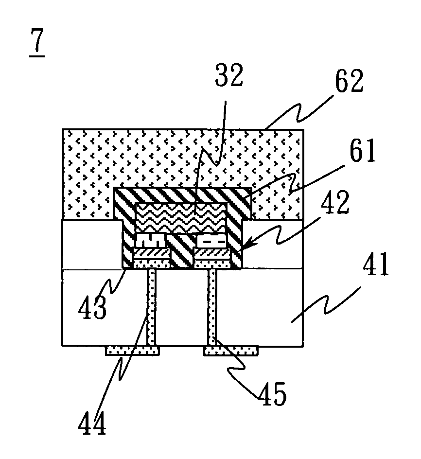
[0043]Step S21: providing a substrate 31;

[0044]Step S22: forming at least one light emitting diode structure 32 on the substrate 31;

[0045]Step S23: providing a package carrier 41 that installs at least one package unit 42, and at least two through holes 44 disposed on the package carrier 41 and corresponding to the package unit 42;

[0046]Step S24: disposing a conducting material 45 into the through holes 44, and forming the conducting material 45 on the package unit 42;

[0047]Step S25: flipping the substrate 31 having the light emitting diode structure 32 over, such that the light emitting diode structure 32 corresponds to the package unit 42 of the package carrier 41;

[004...


PUM


Abstract

This invention discloses a light emitting diode, a wafer level package method, a wafer level bonding method, and a circuit structure for a wafer level package. The light emitting diode includes a package carrier, a conducting material, at least one light emitting diode structure and a package material. The package carrier has at least one package unit and two through holes on the package carrier and corresponding to the package unit. The conducting material is disposed in the through holes and formed at the bottom of the package unit. The light emitting diode structure is formed on a substrate. The substrate having a light emitting diode structure is flipped over in the package unit, and the electrodes of the light emitting diode structure are bonded with the conducting material. After the substrate is removed, a package material is stuffed in the package unit or on the light emitting diode structure.

Description

BACKGROUND OF THE INVENTION[0001]1. Field of the Invention[0002]The present invention relates to a light emitting diode, and more particularly to a light emitting diode that grows a light emitting diode structure onto a substrate, and uses the substrate as a medium for bonding the light emitting diode structure onto a package carrier to achieve the purpose of producing a light emitting diode with a wafer level package.[0003]2. Description of the Related Art[0004]Referring to FIG. 1 for a schematic view of a conventional surface mount device (SMD) type light emitting diode (LED) package, the SMD-type light emitting diode package structure 1 comprises a cup base 12, a conductive lead frame 13, a light emitting diode structure 11, two conductive wires 14 and 15, and an encapsulation 16, wherein the light emitting diode structure 11 is a semiconductor component that luminesces by an external voltage and includes a p-electrode and an n-electrode and connects two conductive wires 14 and 1...

Claims


Application Information

Patent Timeline
Patent Type & Authority Applications(United States)
IPC IPC(8): H01L21/00H01L33/00H01L33/48H01L33/62H01L33/64
CPCH01L2224/48247H01L2924/13034H01L2924/01322H01L2924/19041H01L33/005H01L33/486H01L33/62H01L33/641H01L2224/48091H01L2924/01079H01L2924/00014
Inventor JONG, CHARNG-SHYANGHSU, MING-SENKU, CHIN-FUCHEN, CHIH-MINGHWANG, DENG-HUEI
Owner EPILEDS TECH
Why Eureka
Try Eureka