Cylindrical channel charge trapping devices with effectively high coupling ratios

a charge trapping and cylindrical channel technology, applied in the field of flash memory cells, can solve the problems of inability to apply gate devices, the efficiency of charge trapping memory cells with dielectric charge trapping structures, and the decrement of floating gate technology, etc., and achieve the effect of improving the coupling ratio engineering known from floating gate technology

Active Publication Date: 2008-05-01
MACRONIX INT CO LTD
View PDF20 Cites 63 Cited by
  • Summary
  • Abstract
  • Description
  • Claims
  • Application Information

AI Technical Summary

Benefits of technology

[0015]Other aspects and advantages of the present invention can be seen on review of the drawings, the detailed description and the claims, which follow.

Problems solved by technology

Although this technology has been widely successful, as the sizes of the memory cells and the distances between them shrink, the floating gate technology starts to degrade because of interference between neighboring floating gates.
However, because the charge trapping layer is not conductive, the series capacitor model of floating gate devices does not apply.
The program / erase efficiency of a charge trapping memory cell with a dielectric charge trapping structure, like a SONOS-type device, cannot be improved by the coupling ratio engineering known from the floating gate technology.

Method used


Image

  • Cylindrical channel charge trapping devices with effectively high coupling ratios
  • Cylindrical channel charge trapping devices with effectively high coupling ratios
  • Cylindrical channel charge trapping devices with effectively high coupling ratios

Examples


Embodiment Construction

[0032]A detailed description of various embodiments is provided with reference to FIGS. 1-16.

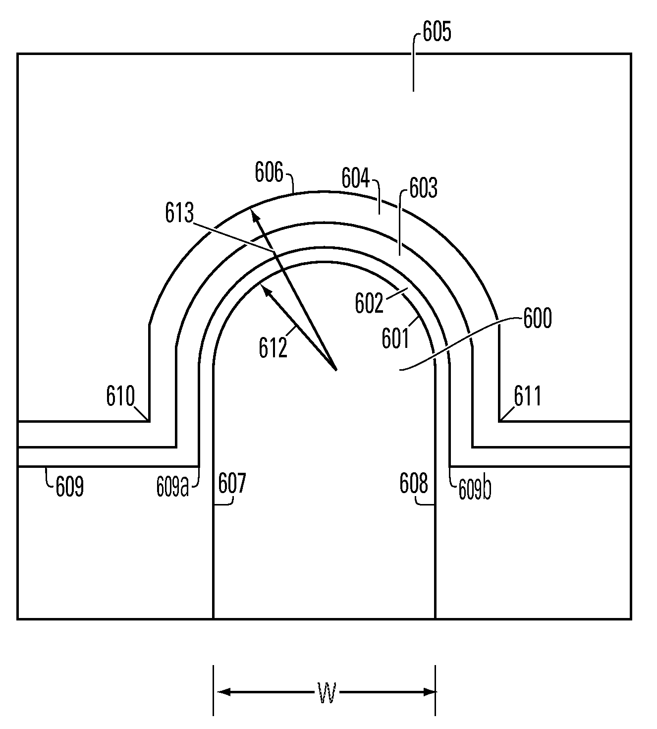
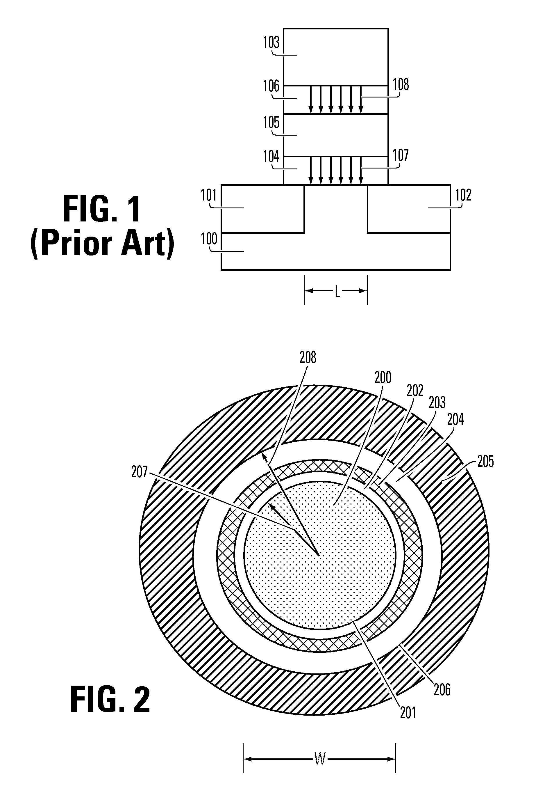
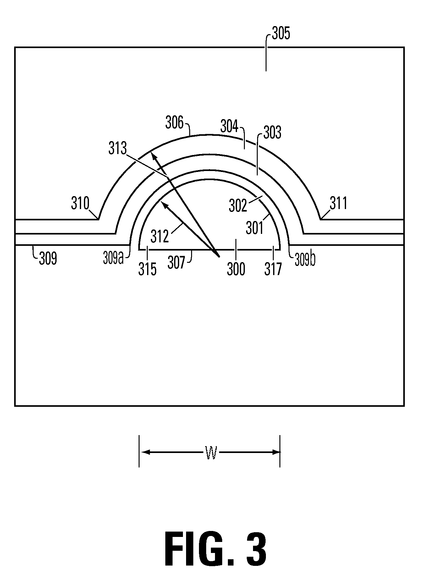
[0033]FIG. 1 illustrates the basic structure of a prior art SONOS-type memory cell. The memory cell is formed on a semiconductor substrate 100 in which a first doped region 101 acts as a source region and a second doped region 102 acts as a drain region. The channel of the memory cell is the region of the substrate 100 between the source region 101 and the drain region 102. A conductive layer 103 is formed over a multi-layer dielectric structure which includes a first dielectric 104, a dielectric charge trapping structure 105, and a second dielectric 106. The dimension L shown in FIG. 1 is typically referred to as the channel length L because current flows between the source region 101 and the drain region 102. In a planar device as shown in FIG. 1, the charge trapping structure is stacked over a flat surface over the channel. The cross-section shown in FIG. 1 is taken in the gate length dir...


PUM


Abstract

A memory cell comprising: a source region and a drain region separated by a semiconductor channel region, the channel region having a channel surface having an area A1 including a first cylindrical region, a first dielectric structure on the channel surface, a dielectric charge trapping structure on the first dielectric structure, a second dielectric structure on the dielectric charge trapping structure, a conductive layer having a conductor surface having an area A2 including a second cylindrical region on the second dielectric structure, the conductor surface overlying the dielectric charge trapping structure and the channel surface of the channel region, and the ratio of the area A2 to the area A1 being greater than or equal to 1.2 are described along with devices thereof and methods for manufacturing.

Description

RELATED APPLICATIONS[0001]This application claims the benefit of U.S. Provisional Application No. 60 / 863,861 filed 1 Nov. 2006, which is hereby incorporated by reference into this application.BACKGROUND OF THE INVENTION[0002]1. Field of the Invention[0003]The invention relates generally to non-volatile memory devices, and in particular to flash memory cells and manufacturing of flash memory devices.[0004]2. Description of Related Art[0005]Flash memory technology includes memory cells that store charge between the channel and gate of a field effect transistor. The charge stored affects the threshold of the transistor, and the changes in threshold due to the stored charge can be sensed to indicate data.[0006]One type of charge storage memory cell in widespread application is known as a floating gate memory cell. In a floating gate memory cell, a tunnel dielectric is formed over a semiconductor channel, a floating gate of conductive material such as polysilicon is formed over the tunne...

Claims


Application Information

Patent Timeline
Patent Type & Authority Applications(United States)
IPC IPC(8): H01L29/792H01L21/336
CPCG11C16/0466H01L21/28282H01L29/0657H01L29/4234H01L29/7926H01L29/7851H01L29/7854H01L29/792H01L29/66833H01L29/40117H01L21/31144
Inventor LUE, HANG-TINGHSU, TZU-HSUAN
Owner MACRONIX INT CO LTD
Why Eureka
Try Eureka