Oxidizing-dephlegmation-based silicon-based wrap gate transistor with buried-channel structure and preparation method thereof

A transistor, silicon-based technology, applied in the field of buried-channel structure silicon-based gate-surrounding transistors, can solve the problems of reducing carrier mobility, random telegraph noise, aggravating carrier scattering noise, etc. The effect of increasing the transmission speed and improving the mobility

Active Publication Date: 2011-08-17
SEMICONDUCTOR MANUFACTURING INTERNATIONAL (BEIJING) CORP +1
View PDF3 Cites 13 Cited by
  • Summary
  • Abstract
  • Description
  • Claims
  • Application Information

AI Technical Summary

Problems solved by technology

[0003] However, an unavoidable problem of silicon-based gate-enclosed devices is the multi-orientation of the channel. The dangling bonds generated by the multi-orientation increase the density of traps and also aggravate carrier scattering and random telegraphy. Noise phenomenon (RTN: Random-Telegraph-Noise)
When carriers flow through the surface channel, the carriers will be attracted or repelled by the trapped charges, changing the transport direction, reducing the mobility of the carriers, thereby reducing the transport speed in the channel

Method used


Image

  • Oxidizing-dephlegmation-based silicon-based wrap gate transistor with buried-channel structure and preparation method thereof
  • Oxidizing-dephlegmation-based silicon-based wrap gate transistor with buried-channel structure and preparation method thereof
  • Oxidizing-dephlegmation-based silicon-based wrap gate transistor with buried-channel structure and preparation method thereof

Examples


Embodiment Construction

[0039] Below in conjunction with accompanying drawing and specific embodiment the present invention is described in further detail:

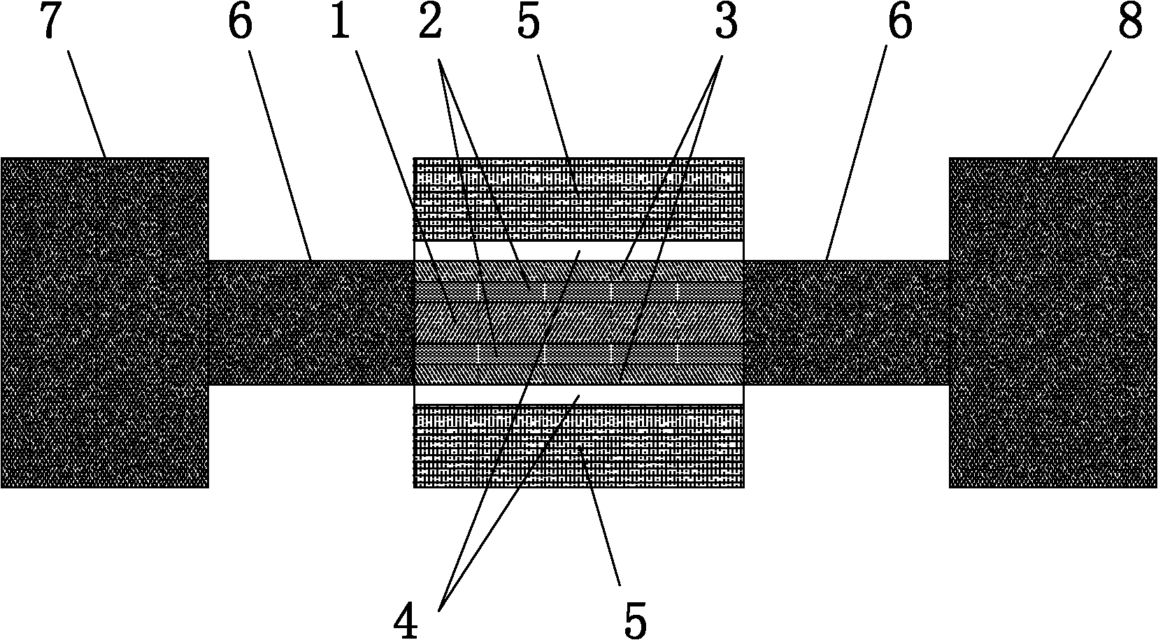
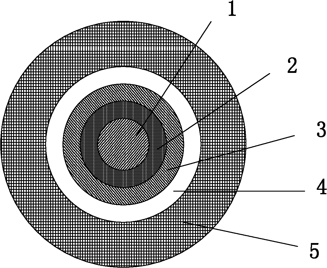
[0040] Figure 1 Knot The structure is a top cross-sectional schematic view of the core part of the buried trench structure silicon-based surrounding gate transistor based on the oxidation segregation technology introduced in the present invention. Its structure is different from the general conventional silicon-based surrounding gate transistors in that:

[0041] The channel is divided into three layers: the channel area, the upper layer of the channel area, and the lower layer of the channel area. These three layers form a buried trench structure that keeps the carrier flow path away from the silicon-silicon dioxide interface. Thus, the influence of the traps at the silicon-silicon dioxide interface on the carriers is reduced. At the same time, the influence of surface roughness on the mobility is avoided.

[0042] Its structure is differe...


PUM

PropertyMeasurementUnit
Thicknessaaaaaaaaaa
Diameteraaaaaaaaaa

Abstract

The invention provides a silicon-based wrap gate transistor with a buried-channel structure, and belongs to the field of electronic semiconductor devices. The transistor comprises a channel region, a gate medium, a gate region, a source region, a drain region and a source/drain terminal epitaxial region, wherein the channel region has a silicon nanowire structure with three layers, a cylindrical channel region lower layer is arranged inside the channel region, and the channel region and the channel region upper layer are wrapped outside the channel region lower layer respectively; impurities with opposite types are mixed into the channel region upper layer and the channel region lower layer; a layer of gate medium region is covered outside the channel region upper layer; and the gate region is positioned on the outer layer of the gate medium. In a preparation method, the silicon-based wrap gate transistor with the buried-channel structure which is suitable to be applied to high-speed circuits is prepared on the basis of an oxidizing dephlegmation technology, so that the phenomena of descending in mobility and serious random telegraph noise which are caused by the polycrystal orientation of wrap gate devices are avoided.

Description

technical field [0001] The invention relates to gate-enclosed field-effect transistors in the field of microelectronic semiconductor devices, in particular to a silicon-based gate-enclosed transistor with buried trench structure suitable for high-speed and low-power consumption circuits based on oxidation segregation technology. Background technique [0002] With the continuous reduction of cost, increase of integration, and improvement of performance of VLSI, the feature size of CMOS devices is continuously reduced, and the leakage current of devices is increasing, and the short-channel effect (SCE: Short-Channel-Effect) is becoming more and more serious. In order to overcome the main problem that hinders the shrinking of the device size, one of the effective ways is to use the multi-gate structure to improve the control ability of the gate to the channel, improve the device characteristics, and make the device better adapt to the small size field. Multi-gate device structu...

Claims


Application Information

Patent Timeline
IPC IPC(8): H01L29/78H01L21/336H01L29/10
Inventor 邹积彬黄如王润声杨庚雨艾玉洁樊捷闻
Owner SEMICONDUCTOR MANUFACTURING INTERNATIONAL (BEIJING) CORP
Why Eureka
Try Eureka