[0003] An
advantage of the invention is to provide an electrooptic device that serves as a display and as an information gathering device. Specifically, an
advantage of the invention is to provide an electrooptic device that allows detection of a position specified on its display screen as well as allows
handwriting thereon while having a simple configuration, for use in an electronic apparatus such as
electronic paper.
[0004] According to a first aspect of the invention, an electrooptic device having an
image display period and an information gathering period includes a panel unit and a
data processing unit. The panel unit includes a first substrate, a second substrate, an electrooptic material interposed between the first and second substrates, a plurality of first scan lines provided above the first substrate, a plurality of second scan lines provided above the first substrate and disposed in parallel to the first scan lines, a plurality of
signal lines provided above the first substrate and intersecting the first scan lines and the second scan lines, and a plurality of pixels provided above the first substrate and disposed at intersections of the first scan lines and the second scan lines and
signal lines. Each pixel located in an i-th row and a j-th column (i and j are both natural numbers) includes a first transistor, a second transistor, and a pixel
electrode. The plurality of pixels are formed in a matrix on the first substrate. A gate of the first transistor is coupled to the first
scan line in the i-th row. One of a source and a drain of the first transistor is coupled to the signal line on the j-th column. A gate of the second transistor is coupled to the second scan line in the i-th row. One of a source and a drain of the second transistor is coupled to the other of the source and drain of the first transistor. The other of the source and drain of the first transistor is coupled to the pixel electrode.
[0005] In the electrooptic device according to the first aspect of the invention, the other of the source and drain of the second transistor may be coupled to a reference power supply. Since the first scan line in an (i−1)-th row may be used as the reference power supply, the other of the source and drain of the second transistor may be coupled to the first scan line in the (i−1)-th row. In the electrooptic device according to the first aspect of the invention, the panel unit may further include a holding
capacitance provided between the other of the source and drain of the first transistor and the reference power supply. If the first scan line in the (i−1)-th row is used as the reference power supply, the panel unit may include a holding
capacitance provided between the other of the source and drain of the first transistor and the reference power supply and the first scan line in the (i−1)-th row.
[0006] In the electrooptic device according to the first aspect of the invention, the panel unit may further include a common electrode disposed on the second substrate and a light shielding film disposed between the first substrate and the second transistor. The first substrate may be transparent. The pixel electrode may be formed of a transparent conductive film. If the panel unit includes the holding
capacitance, it may further include a common electrode disposed on the second substrate and a light shielding film disposed between the first substrate and the second transistor as described above. The first substrate may be transparent. The pixel electrode may be formed of a transparent conductive film. The holding capacitance may include a holding capacitance first electrode, a holing capacitance second electrode, and a holding capacitance
dielectric film interposed therebetween. The holding capacitance first and second electrodes and the holding capacitance
dielectric film may be all transparent. The pixel electrode may also serve as the holding capacitance second electrode. The light shielding film may be provided in a position that overlaps an active region of the second transistor. The light shielding film may be provided in a position that does not overlap an active region of the first transistor.
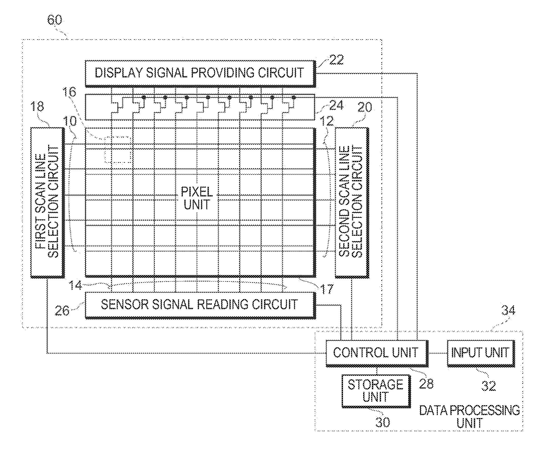
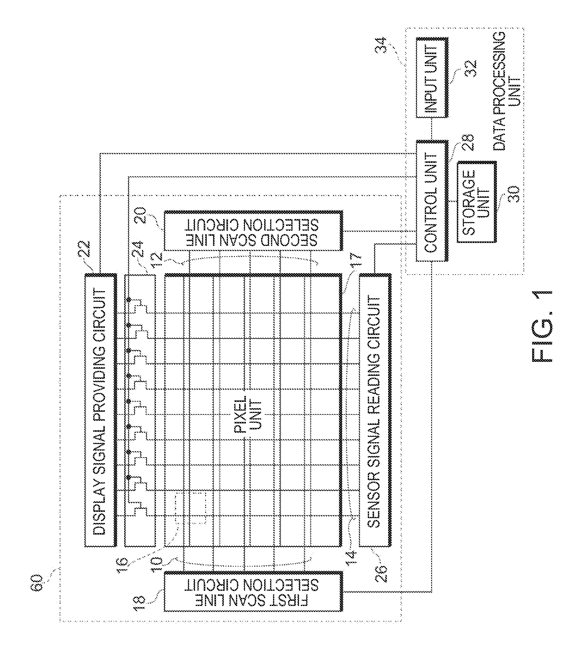
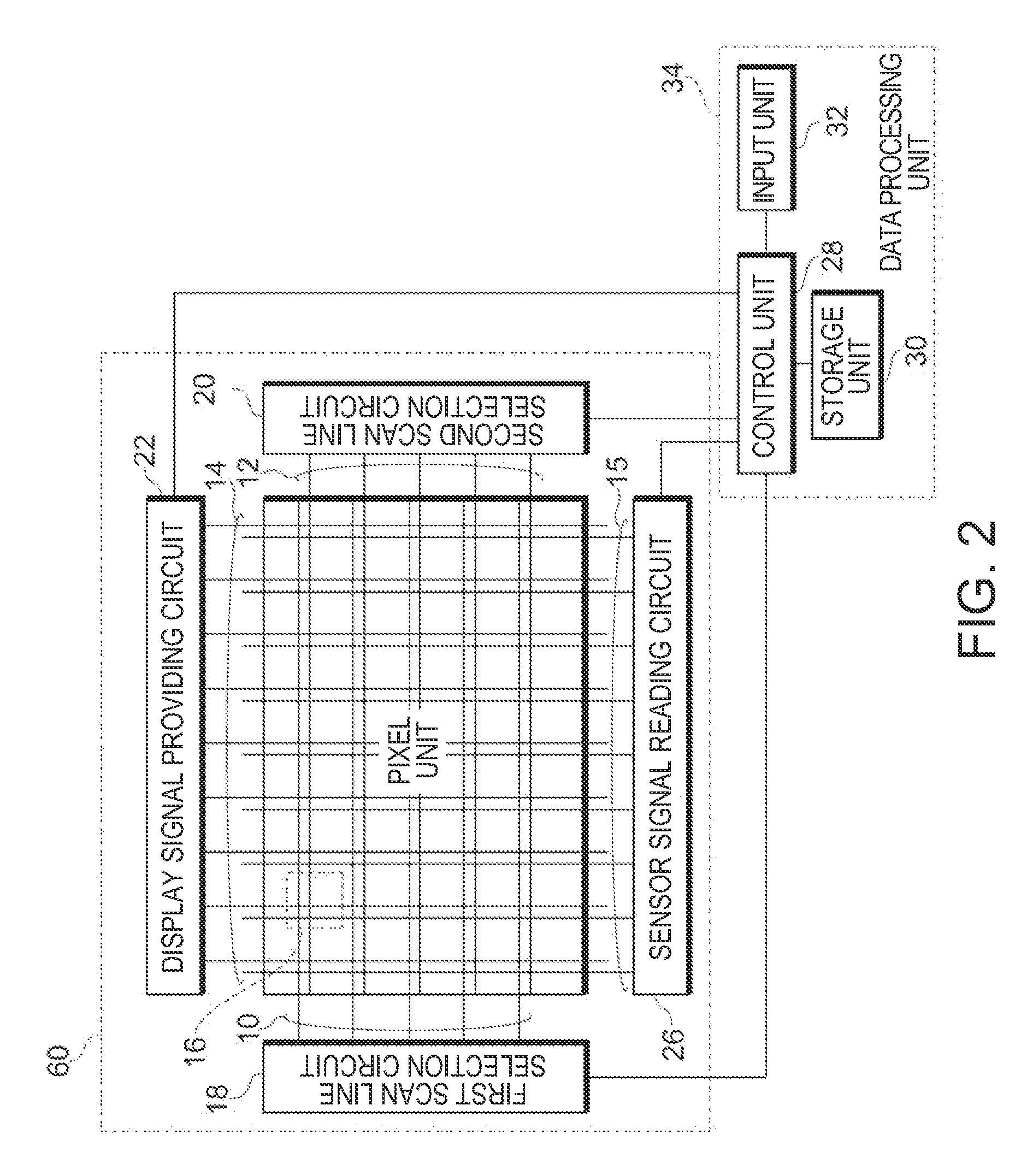
[0007] In the electrooptic device according to the first aspect of the invention, the panel unit may further include a first scan selection circuit coupled to the first scan lines and serving to select a particular one from among the plurality of first scan lines, a second scan selection circuit coupled to the second scan lines and serving to select a particular one from among the plurality of second scan lines, a display signal providing circuit coupled to first ends of the
signal lines and serving to supply to each signal line a display signal that is unique to each signal line, and a sensor signal reading circuit coupled to second ends of the signal lines and serving to read a sensor signal outputted from each signal line and unique to each signal line, all of which are disposed on the first substrate. In the electrooptic device according to the first aspect of the invention, the
data processing unit may include an input unit, a
control unit, and a storage unit. The input unit may serve to supply display image information inputted from outside to the
control unit or the storage unit. The
control unit may serve to control at least the first scan selection circuit, the second scan selection circuit, the display signal providing circuit, the sensor signal reading circuit, and the storage unit. The storage unit may serve to store the display image information and write image information based on the sensor signal. The control unit may serve to create a new display image using the display image information and the write image information and to supply the new display image as a new display signal to the display signal providing circuit. In the electrooptic device according to the first aspect of the invention, the panel unit may further include a switching circuit disposed between the signal lines and the display signal providing circuit for switching between continuity and discontinuity between the signal lines and the display signal providing circuit. The switching circuit may provide continuity between the signal lines and the display signal providing circuit during the
image display period. It may provide discontinuity between the signal lines and the display signal providing circuit during the information gathering period.
[0008] In the electrooptic device according to the first aspect of the invention, the electrooptic material may be an electrophoretic material, a
liquid crystal material, or an electrochromic material.
