CMOS device with raised source and drain regions

a technology of metal oxidesemiconductor and source, applied in the direction of semiconductor devices, electrical apparatus, transistors, etc., can solve the problems of difficult control of implantation depth for forming shallow junctions in source and drain extension regions of small-scale devices, process incurs several problems, and the effect of reducing the implantation depth

Active Publication Date: 2008-05-01
TAIWAN SEMICON MFG CO LTD
View PDF25 Cites 50 Cited by
  • Summary
  • Abstract
  • Description
  • Claims
  • Application Information

AI Technical Summary

Benefits of technology

[0010]In accordance with yet another aspect of the present invention, a semiconductor structure includes a semiconductor substrate comprising a PMOS device in a PMOS region and an NMOS device in an NMOS region. The PMOS device includes a first gate stack on the semiconductor substrate; a first offset spacer on a sidewall of the first gate stack; a stressor in the semiconductor substrate and having a portion under the first offset spacer; a first raised source / drain extension region on the stressor and adjoining the first offset spacer, wherein the first raised source / drain extension region has at least a portion higher than a top surface of the semiconductor substrate; and a first main spacer on a sidewall of the first offset spacer, wherein the first main spacer has at least a portion on a top surface of the first raised source / drain extension region. The NMOS device includes a second gate stack on the semiconductor substrate; a second offset spacer on a sidewall of the second gate stack; a second raised source / drain extension region on the semiconductor substrate and adjoining the second offset spacer; a second main spacer on a sidewall of the second offset spacer, wherein the second main spacer has at least a portion on a top surface of the second raised source / drain extension region; and a deep source / drain region adjoining the second raised source / drain extension region, wherein a portion of the deep source / drain region, that is lower than a top surface of the semiconductor substrate, is free from stressors.

Problems solved by technology

This reduction causes technical difficulties during the formation processes.
Controlling implantation depth for forming shallow junction in source and drain extension regions of small-scale devices is also difficult.
This process incurs several problems.
Second, epitaxial growth of silicon typically requires high temperatures, and thus excessive diffusion of dopant degrades short channel performance of the MOS devices.
Further drawbacks include low activation rates and low solubilities (since impurities are implanted), and high silicide contact resistance, which results from the low activation rates and low solubilities of impurities.

Method used


Image

  • CMOS device with raised source and drain regions
  • CMOS device with raised source and drain regions
  • CMOS device with raised source and drain regions

Examples


Embodiment Construction

[0015]The making and using of the presently preferred embodiments are discussed in detail below. It should be appreciated, however, that the present invention provides many applicable inventive concepts that can be embodied in a wide variety of specific contexts. The specific embodiments discussed are merely illustrative of specific ways to make and use the invention, and do not limit the scope of the invention.

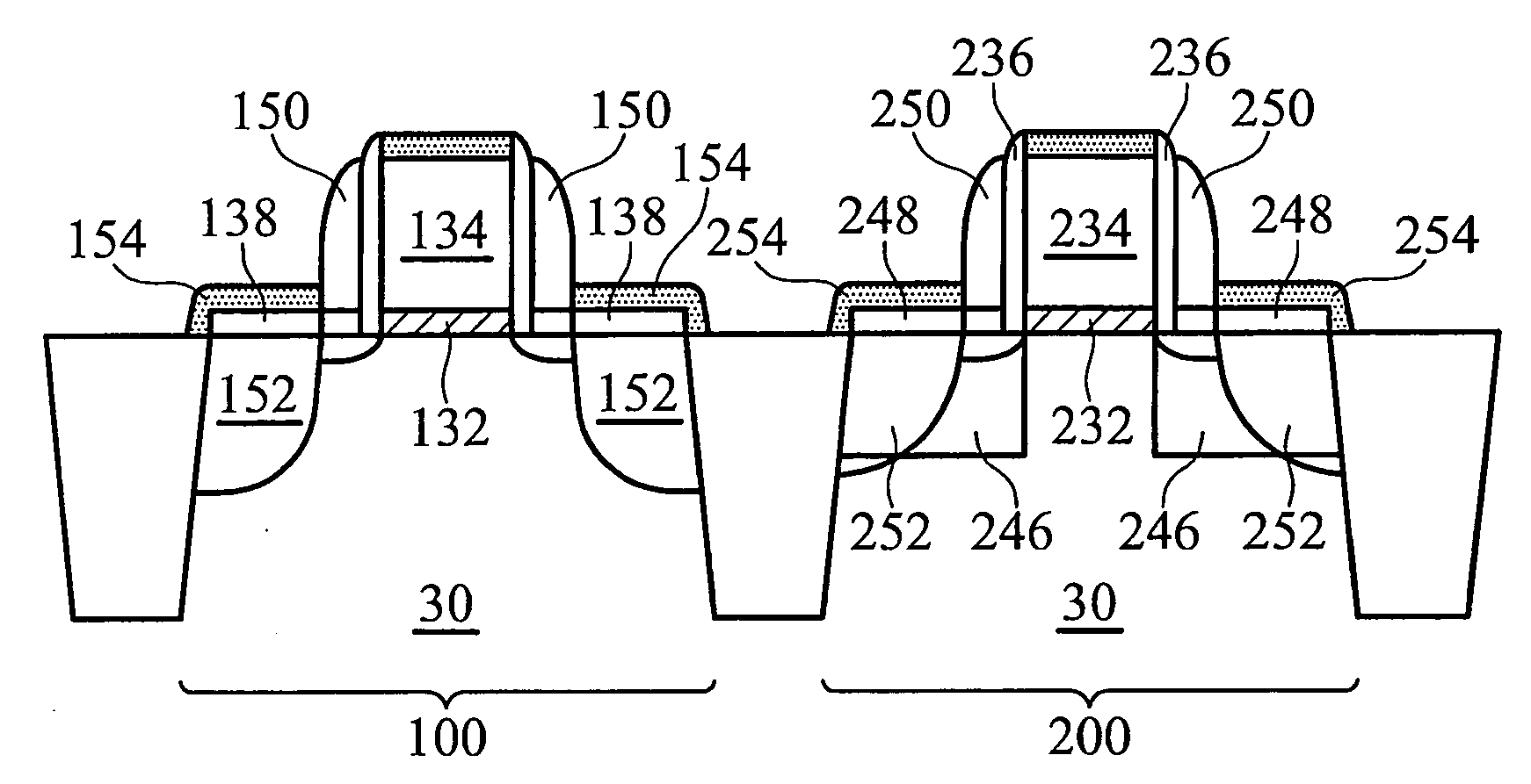
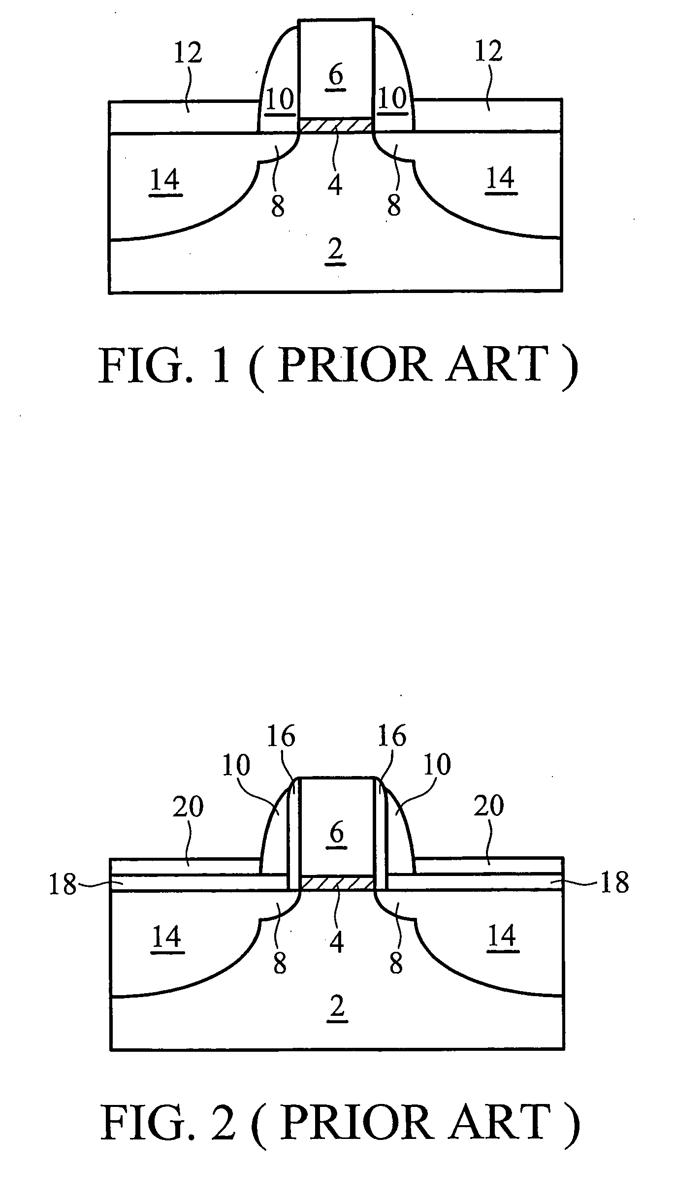
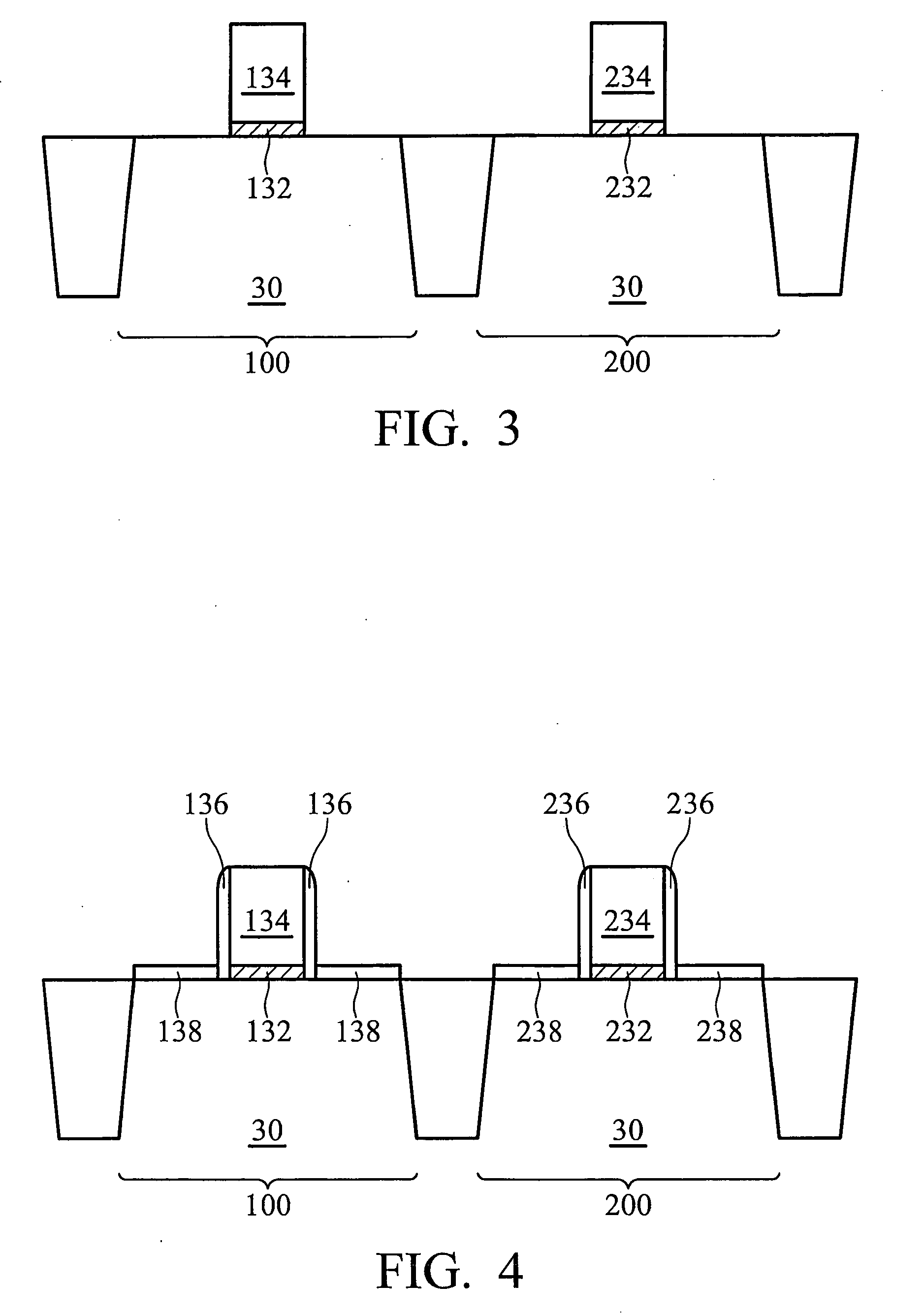
[0016]Research results have revealed that solubilities of impurities in source and drain regions of metal-oxide-semiconductor (MOS) devices are related to the strain in the source and drain regions. Typically, p-type impurities, such as boron, have improved solubility under compressive strains. N-type impurities, such as arsenic, have improved solubility under tensile strains. However, further research results have revealed that the improvement in solubility of arsenic under tensile strain is significantly less than the improvement in solubility of boron under compressive str...


PUM


Abstract

A method of forming a semiconductor structure includes forming a PMOS device and an NMOS device. The step of forming the PMOS device includes forming a first gate stack on a semiconductor substrate; forming a first offset spacer on a sidewall of the first gate stack; forming a stressor in the semiconductor substrate using the first offset spacer as a mask; and epitaxially growing a first raised source/drain extension (LDD) region on the stressor. The step of forming the NMOS device includes forming a second gate stack on the semiconductor substrate; forming a second offset spacer on a sidewall of the second gate stack; epitaxially growing a second raised LDD region on the semiconductor substrate using the second offset spacer as a mask; and forming a deep source/drain region adjoining the second raised LDD region.

Description

TECHNICAL FIELD[0001]This invention relates generally to semiconductor devices, and more particularly to metal-oxide-semiconductor (MOS) devices with raised source and drain regions.BACKGROUND[0002]With the scaling of integrated circuits, metal-oxide-semiconductor (MOS) devices become increasingly smaller. The junction depths of the MOS devices are also reduced accordingly. This reduction causes technical difficulties during the formation processes. For example, small MOS devices demand higher dopant concentrations in source and drain regions in order to reduce resistivity in the source and drain regions. Controlling implantation depth for forming shallow junction in source and drain extension regions of small-scale devices is also difficult.[0003]To solve the above-discussed problems, raised source and drain regions and / or raised lightly doped source and drain (LDD) regions have been formed. FIG. 1 illustrates a commonly formed MOS device having raised source / drain regions. In its ...

Claims


Application Information

Patent Timeline
Patent Type & Authority Applications(United States)
IPC IPC(8): H01L21/8238
CPCH01L21/823814H01L27/092H01L29/165H01L29/7848H01L29/66628H01L29/66636H01L29/7834H01L29/665
Inventor LIANG, CHUN-SHENGCHEN, HUNG-MINGHUANG, CHIEN-CHAOYANG, FU-LIANG
Owner TAIWAN SEMICON MFG CO LTD
Why Eureka
Try Eureka