Timing failure remedying apparatus for an integrated circuit, timing failure diagnosing apparatus for an integrated circuit, timing failure diagnosing method for an integrated circuit, integrated circuit, computer readable recording medium recorded thereon a timing failure diagnosing program for an integrated circuit, and computer readable recording medium recorded thereon a timing failure remedying program for an integrated circuit

a timing failure and remedying technology, applied in the field of timing failure remedying apparatus for integrated circuits, can solve problems such as increased test time, increased flip-flips on the lsi, and longer scan shift tim

Inactive Publication Date: 2008-05-01
FUJITSU LTD
View PDF6 Cites 11 Cited by
  • Summary
  • Abstract
  • Description
  • Claims
  • Application Information

AI Technical Summary

Benefits of technology

[0043]Further, when the diagnosing unit pronounces a timing failure, the adjuster adjusts at least either the second cycle or a delay amount of the second clock signal in order to remedy the timing fa...

Problems solved by technology

In the recent LSI, the gate scale is very large, which causes an increase in number of flip-flips on the LSI.
This leads to a longer scan shift time, which causes an increase in test time.
This further causes problems with the test cost and TAT (Turn Around Time).
Thus, the effect of parallelization of the scan chains cannot be obtained.
However, the known logic BIST cannot detect a position of the timing failure, thus cannot...

Method used


Image

  • Timing failure remedying apparatus for an integrated circuit, timing failure diagnosing apparatus for an integrated circuit, timing failure diagnosing method for an integrated circuit, integrated circuit, computer readable recording medium recorded thereon a timing failure diagnosing program for an integrated circuit, and computer readable recording medium recorded thereon a timing failure remedying program for an integrated circuit
  • Timing failure remedying apparatus for an integrated circuit, timing failure diagnosing apparatus for an integrated circuit, timing failure diagnosing method for an integrated circuit, integrated circuit, computer readable recording medium recorded thereon a timing failure diagnosing program for an integrated circuit, and computer readable recording medium recorded thereon a timing failure remedying program for an integrated circuit
  • Timing failure remedying apparatus for an integrated circuit, timing failure diagnosing apparatus for an integrated circuit, timing failure diagnosing method for an integrated circuit, integrated circuit, computer readable recording medium recorded thereon a timing failure diagnosing program for an integrated circuit, and computer readable recording medium recorded thereon a timing failure remedying program for an integrated circuit

Examples


first embodiment

[1] First Embodiment of the Invention

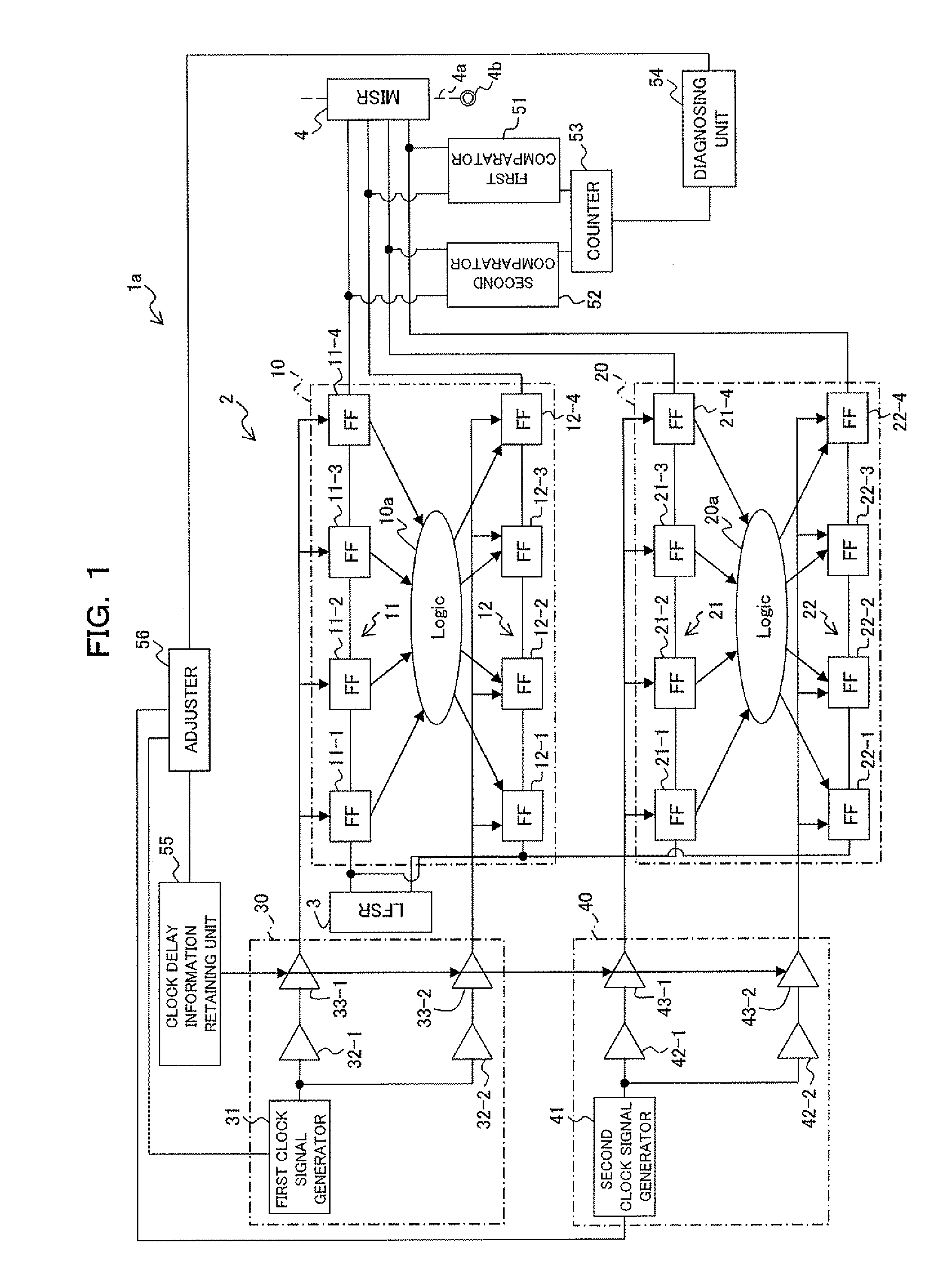
[0067]First, description will be made of a structure of a timing failure remedying apparatus for an integrated circuit according to a first embodiment of this invention, with reference to FIG. 1. As shown in FIG. 1, the timing failure remedying apparatus for an integrated circuit 1a according to this embodiment diagnoses and remedies a timing failure in an integrated circuit [for example, an LSI (Large Scale Integration)]2 having a plurality (two, here) of CPU (Central Processing Unit) cores (processing cores) 10 and 20.

[0068]The timing failure remedying apparatus 1a comprises an LFSR (Linear Feedback Shift Register; pattern generator) 3, an MISR (Multiple Input Signature Register) 4, a first clock signal applying unit 30, a second clock signal applying unit 40, a first comparator (comparator) 51, a second comparator 52, a counter 53, a diagnosing unit 54, a clock delay setting information retaining unit (delay amount setting information retainin...

second embodiment

[2] Second Embodiment of the Invention

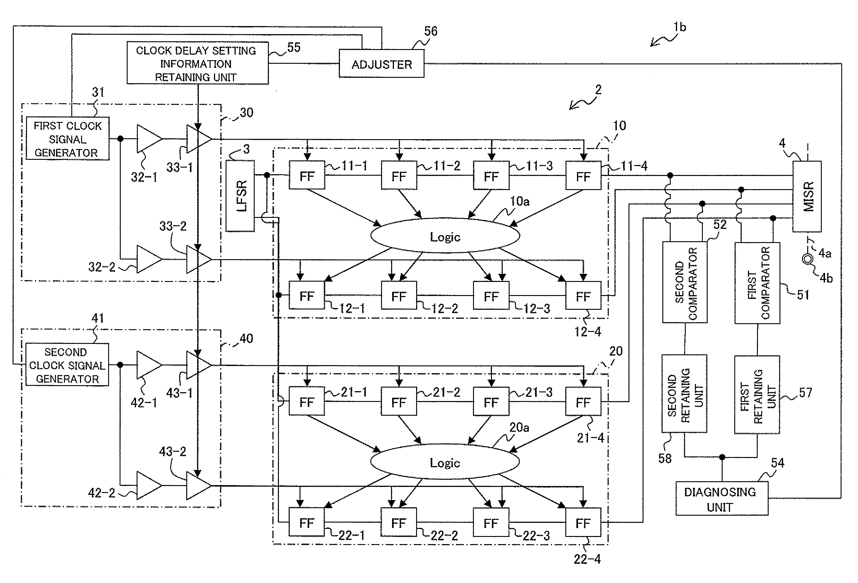
[0146]Next, description will be made of a structure of a timing failure remedying apparatus for an integrated circuit according to a second embodiment of this invention with reference to FIG. 9. As shown in FIG. 9, the timing failure remedying apparatus 1b for an integrated circuit according to this embodiment has the same structure as the timing failure remedying apparatus 1a according to the above-described first embodiment, excepting that the timing failure remedying apparatus 1b has a first retaining unit 57 and a second retaining unit 58 instead of the counter 53 of the first embodiment. Incidentally, like reference characters in FIG. 9 designate like or corresponding parts, detailed descriptions of which are thus omitted here.

[0147]The first retaining unit 57 retains a result of comparison by the first comparator 51. Concretely, the first retaining unit 57 is a flag. When it is determined that an expectation value obtained in the flip-flop...

third embodiment

[3] Third Embodiment of the Invention

[0162]Next, description will be made of a structure of a timing failure remedying apparatus for an integrated circuit according to a third embodiment of this invention with reference to FIG. 11. As shown in FIG. 11, the timing failure remedying apparatus 1c for an integrated circuit according to this embodiment has a similar structure to that of the timing failure remedying apparatus 1a according to the first embodiment, excepting that the timing failure remedying apparatus 1c has an OR gate 59 instead of the above-described counter 53 of the first embodiment, and structures of scan chains 21′ and 22′ are different (more concretely, structures of flip-flops 21-4′ and 22-4′ in the final stage). Incidentally, like reference characters in FIG. 11 designate like or corresponding parts, detailed descriptions of which are thus omitted here.

[0163]The OR gate 59 is inputted thereto results of comparison by both the first comparator 51 and the second comp...


PUM


Abstract

A timing failure remedying apparatus for an integrated circuit has a comparator which compares a value captured in a taking-out scan chain for reference through an operation of a processing core for reference according to a first clock signal with a value captured in a taking-out scan chain to be tested through an operation of a processing core to be tested according to a second clock signal, a diagnosing unit which determines a timing failure in the logic circuit to be tested on the basis of a result of comparison by the comparator, and an adjuster which adjusts at least either a second cycle or a delay amount of the second clock signal. It is possible to examine a position of the timing failure or the number of the timing failures in the integrated circuit diagnosed as that its logic is normal but the timing failure occurs therein.

Description

BACKGROUND OF THE INVENTION[0001]1) Field of the Invention[0002]The present invention relates to a technique for diagnosing / remedying a timing failure in an integrated circuit [for example, an LSI (Large Scale Integration)]. More specifically, the present invention relates to a technique for diagnosing / remedying a timing failure such as over-delay or the like occurring in an LSI having a plurality of same logic circuits [CPU (Central Processing Unit) cores].[0003]2) Description of the Related Art[0004]In order to determine whether an integrated circuit (for example, an LSI) is good or bad, as shown in FIG. 17, good / bad determination of an LSI 104 is carried out in the following manner, in general. In a scan chain 101 formed by connecting a plurality of flip-flops (denoted as “FF” in the drawing) 100-1 through 100-15 (hereinafter denoted simply by a reference character “100” when these flip-flops 100-1 through 100-15 are not specifically discriminated from one another) in series, set...

Claims


Application Information

Patent Timeline
IPC IPC(8): G06F11/22
CPCG01R31/318552G06F11/27G01R31/318594G01R31/318566
Inventor SATSUKAWA, YOSHIHIKO
Owner FUJITSU LTD
Why Eureka
Try Eureka