Electronic Device, a Chip Contacting Method and a Contacting Device

a technology of contact method and contacting device, which is applied in the direction of semiconductor devices, semiconductor/solid-state device details, electrical apparatus, etc., can solve the problem of uncritical compression force applied during the bonding process, and achieve the effect of reliable and stable performance and cost-effectiveness

Inactive Publication Date: 2008-05-08
TEXAS INSTR INC
View PDF6 Cites 4 Cited by
  • Summary
  • Abstract
  • Description
  • Claims
  • Application Information

AI Technical Summary

Benefits of technology

[0008]An aspect of the present invention provides an electronic device which is characterized by a very reliable and stable performance and which can be produced in a very cost-effective manner.

Problems solved by technology

With this space layer the compression force applied during the bonding process becomes uncritical.

Method used


Image

  • Electronic Device, a Chip Contacting Method and a Contacting Device
  • Electronic Device, a Chip Contacting Method and a Contacting Device
  • Electronic Device, a Chip Contacting Method and a Contacting Device

Examples


Embodiment Construction

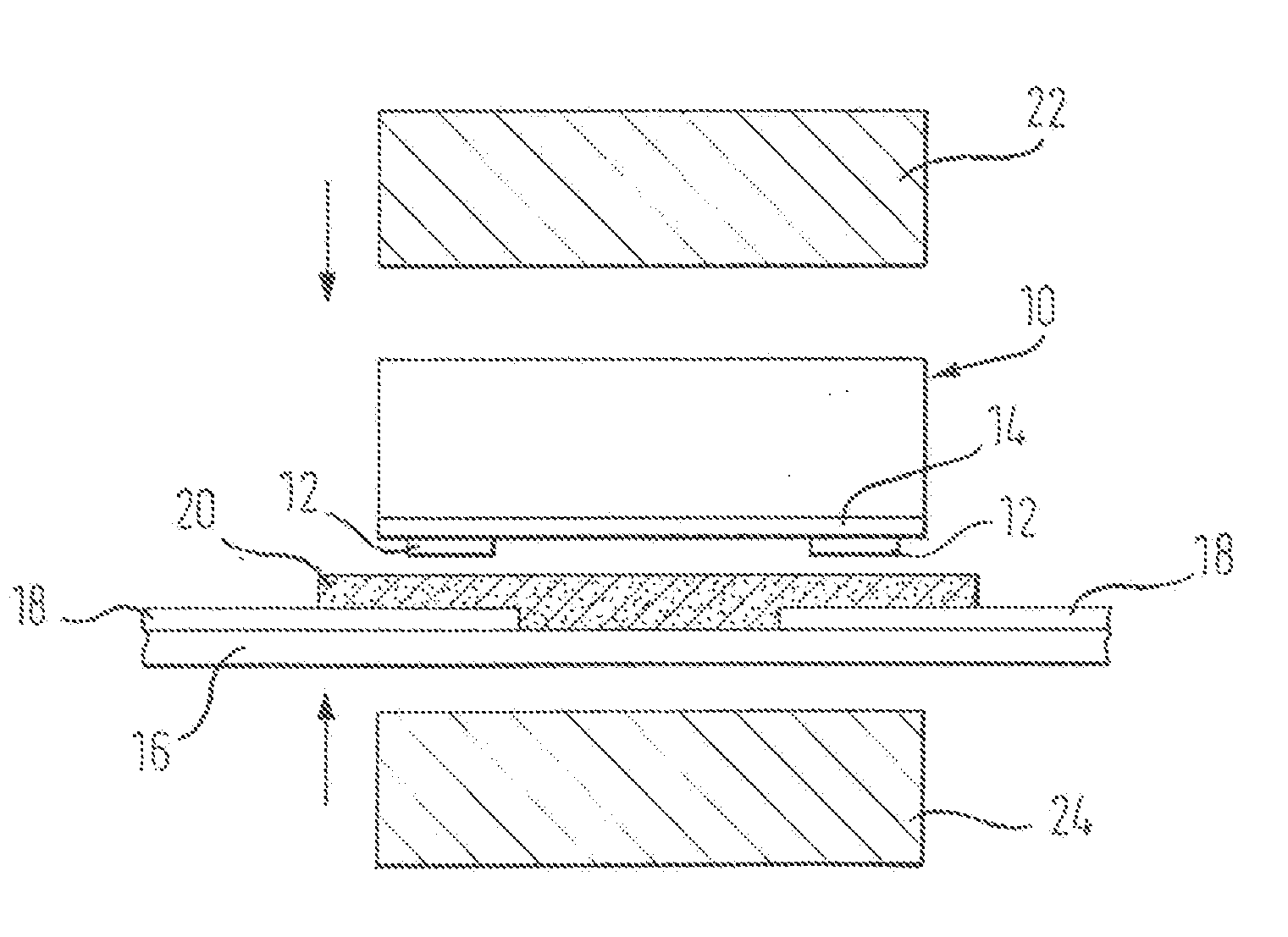
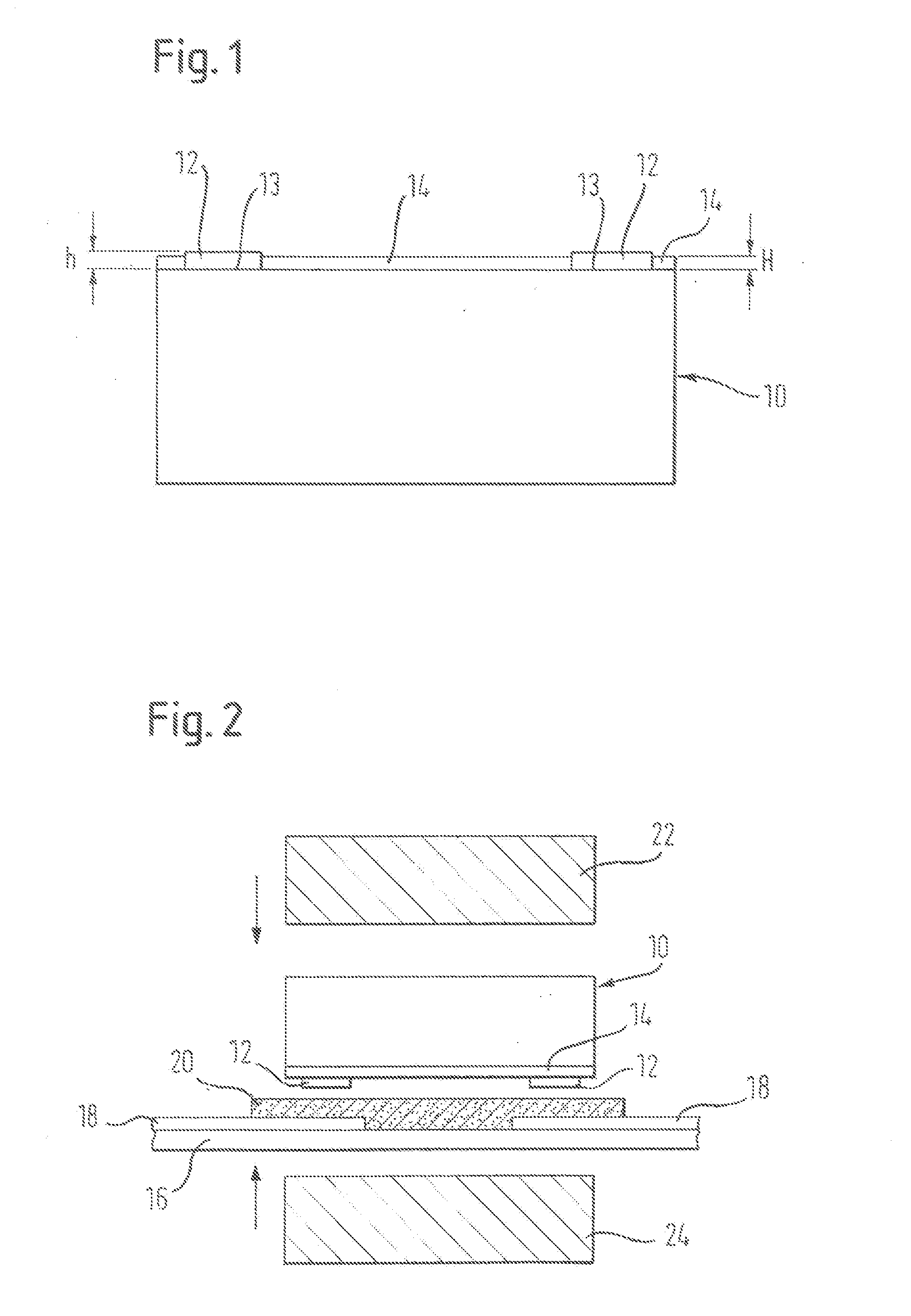
[0022]FIG. 1 shows a chip 10 with a pair of contact bumps 12 for establishing an electrical contact with a conductive structure of a carrier substrate which can be seen in FIG. 2. The contact bumps 12 are deposited on bonding pads 13 of the chip 10 and each have a height h. The surfaces of the contact bumps 12 facing away from the chip 10 are preferably substantially plane. On the same surface of the chip 10 on which the contact bumps 12 are deposited a non-conductive space layer 14 with a thickness H is provided. As can be seen in the FIG. 1, the thickness H of the non-conductive space layer 14 is slightly smaller than the height h of the contact bumps 12 so that the contact bumps 12 slightly protrude from the space layer 14. The difference in the thickness of space layer 14 and the height of the contact bumps 12, i.e. the distance which the contact bumps protrude from the non-conductive space layer 14, is between 3 pin and 12 pm. A typical material which the contact bumps 12 are m...


PUM


Abstract

An electronic device includes a chip (10) and a carrier substrate (16), wherein the carrier substrate (16) has a conductive structure (18) and the chip (10) has a pair of bonding pads (13) on a side facing the carrier substrate (16). The bonding pads (13) are in electrical contact with the conductive structure (18). The chip (10) has a non-reductive space layer (14) on the side facing the carrier substrate (16), wherein the non-conductive space layer (14) defines the distance between the chip (10) and the conductive structure (16) of the carrier substrate (16).

Description

FIELD OF THE INVENTION[0001]The present invention relates generally to an electronic device which comprises a chip and a carrier substrate. The carrier substrate comprises a conductive structure and the chip comprises a pair of bonding pads on a side facing the carrier substrate. The bonding pads are in electrical contact with the conductive structure.[0002]The present invention also relates to a chip contacting method for contacting multiple chips with multiple conductive structures. The multiple conductive structures are arranged on a common carrier substrate.[0003]The present invention further relates to a contacting device for contacting multiple chips with multiple conductive structures, wherein the multiple conductive structures are arranged on a common carrier substrate.BACKGROUND OF THE INVENTION[0004]When an electrical contact is established between the conductive structure of the carrier substrate and a bonding pad of the chip, process control and repeatability are very im...

Claims


Application Information

Patent Timeline
Patent Type & Authority Applications(United States)
IPC IPC(8): H01L23/52
CPCH01L21/563H01L23/3171H01L2224/32225H01L24/75H01L2924/01072H01L2924/01033H01L2924/01005H01L2924/3011H01L2924/01082H01L2924/01079H01L2924/01075H01L2924/01061H01L2924/01047H01L2924/01046H01L2924/01029H01L2924/01013H01L2224/97H01L24/83H01L24/90H01L24/97H01L2224/1147H01L2224/16225H01L2224/73203H01L2224/73204H01L2224/75H01L2224/75251H01L2224/75252H01L2224/75314H01L2224/83192H01L2224/838H01L2924/00H01L2924/00011H01L2924/00014H01L2224/0401
Inventor SCHMID, HERMANNTAN, ENN LEONG
Owner TEXAS INSTR INC
Why Eureka
Try Eureka