System and method for high-energy sputtering using return conductors

Inactive Publication Date: 2008-05-15
APPLIED MATERIALS INC
View PDF5 Cites 0 Cited by
  • Summary
  • Abstract
  • Description
  • Claims
  • Application Information

AI Technical Summary

Benefits of technology

[0012]Exemplary embodiments of the present invention that are shown in the drawings are summarized below. These and other embodiments are more fully described in the Detailed Description section. It is to be understood, however, that there is no intention to limit the invention to the forms described in this Summary of the Invention or in the Detailed Description. One skilled in the art can recognize that there are numerous modifications, equivalents and alternative constructions that fall within the spirit and scope of the invention as expressed

Problems solved by technology

These typical return paths inside the process chamber are problematic for high-power/high-frequency power supplies because the return paths are too resistant to electron flow.
First, skin effects force the electrons to flow along the surface of the inside of the process chamber, thereby reducing the effectiveness of the return path.
And as the frequency of the power supply increases, this skin effect becomes more pronounced and reduces the effectiveness of the return path to unacceptable levels.
Rough surfaces present far more resistance to electron flow than do smooth surfaces, and stainless steel is a poor conductor.
The primary problem with high resistance is

Method used


Image

  • System and method for high-energy sputtering using return conductors
  • System and method for high-energy sputtering using return conductors
  • System and method for high-energy sputtering using return conductors

Examples


Example

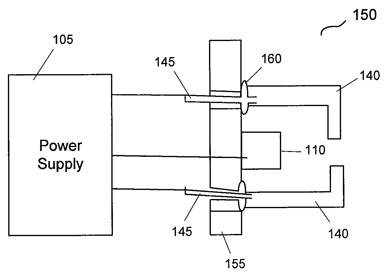
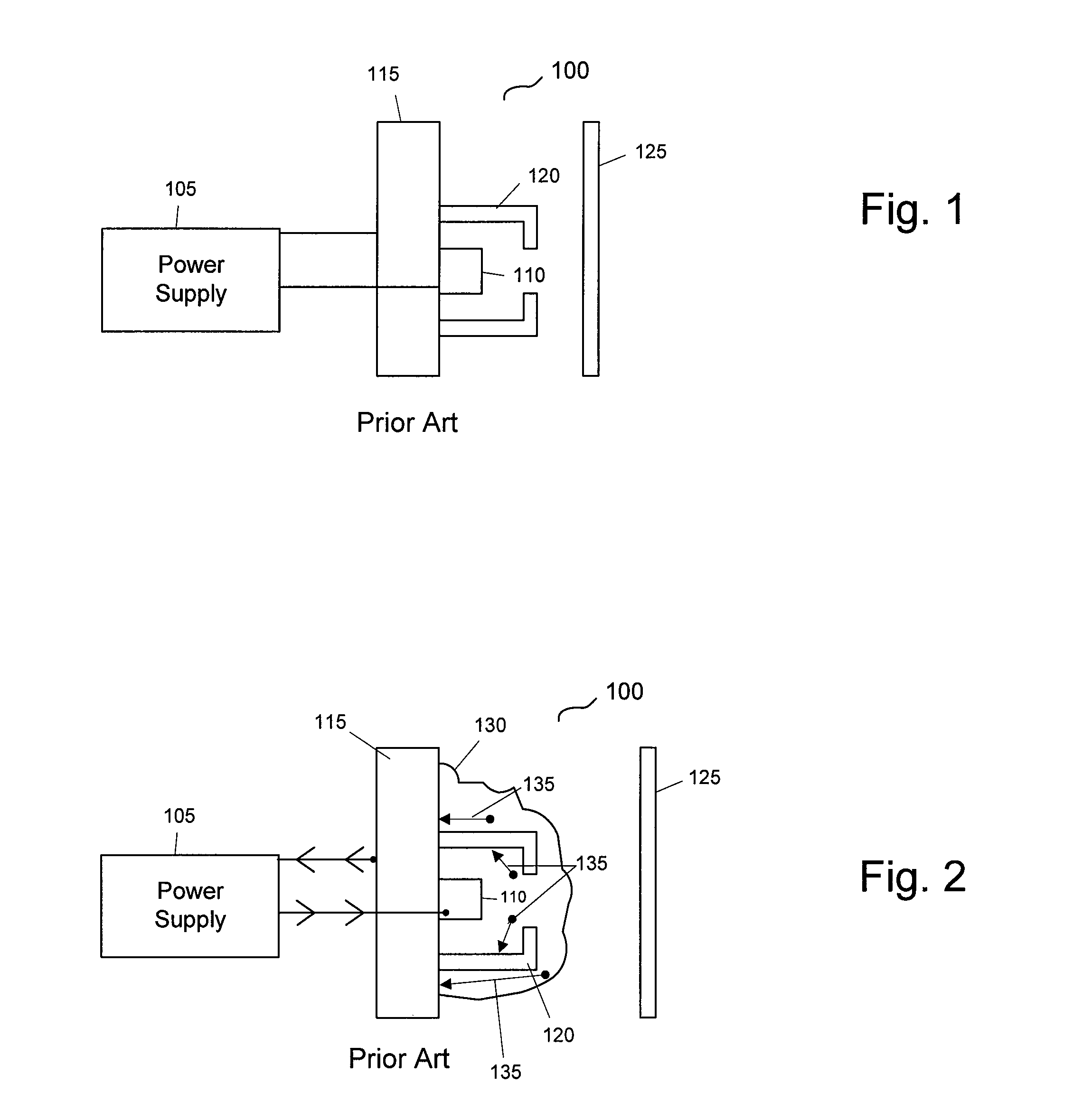
[0023]Referring now to the drawings, where like or similar elements are designated with identical reference numerals throughout the several views, and referring in particular to FIGS. 1 and 2, the illustrate a typical sputter system 100. This system includes a power supply 105. The power supply could be typically a DC, AC, pulsed DC, RF or other power supply. As previously discussed, the power supply 105 could be attached to an impedance matching network, include an integrated impedance matching network, or operate in conjunction with any type of tuning network. For clarity, “impedance matching network” as used in this document includes typical impedance matching networks and any other tuning network.

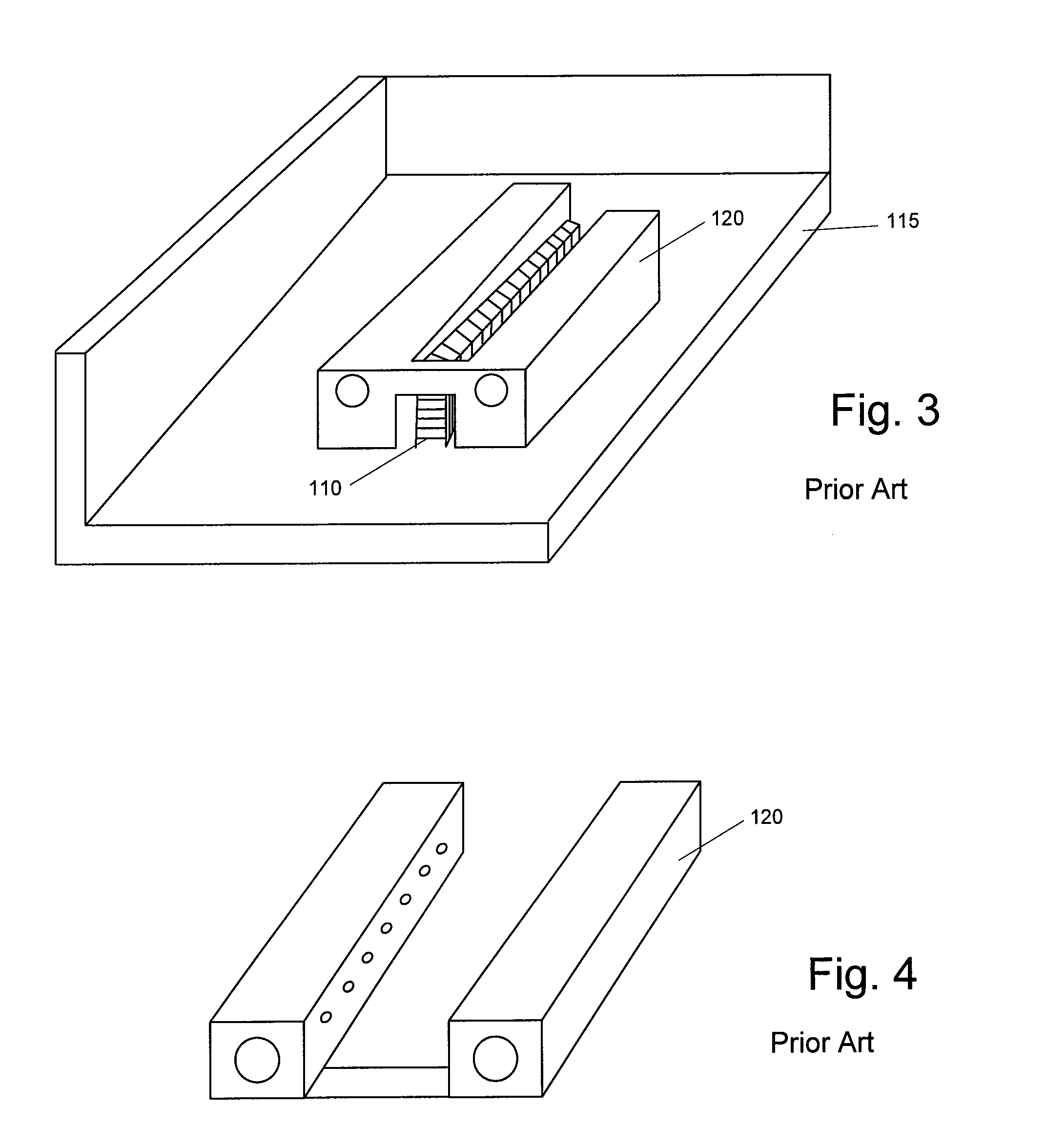
[0024]The power supply 105 is connected to the target 110, which is located inside the process chamber 115. During operation, an inert gas is release around the target 110, preferably through the use of a gas box 120 that helps distribute the gas evenly. The gas box 120 typically partia...


PUM

PropertyMeasurementUnit
Poweraaaaaaaaaa
Electric impedanceaaaaaaaaaa

Abstract

A system and method for sputtering is described. One embodiment includes a sputtering system that includes a vacuum chamber; a gas box secured to the inner surface of the vacuum chamber; a plurality of return conductors engaged with the gas box, the plurality of return conductors extending through the vacuum chamber; and a plurality of seals configured to engage corresponding ones of the plurality of return conductors, the plurality of seal configured to maintain the vacuum inside the vacuum chamber.

Description

COPYRIGHT[0001]A portion of the disclosure of this patent document contains material that is subject to copyright protection. The copyright owner has no objection to the facsimile reproduction by anyone of the patent disclosure, as it appears in the Patent and Trademark Office patent files or records, but otherwise reserves all copyright rights whatsoever.FIELD OF THE INVENTION[0002]The present invention relates to sputtering systems and methods. In particular, but not by way of limitation, the present invention relates to systems and methods for high-energy sputtering using highly-conductive return conductors.BACKGROUND OF THE INVENTION[0003]Sputtering is used in several industries to deposit and adhere material to substrates. For example, sputtering is used extensively in semiconductor, glass, and display manufacturing. Sputtering is well-known in the art and is only described briefly herein. Those of skill in the art are very familiar with this process.[0004]In basic sputtering, ...

Claims


Application Information

Patent Timeline
IPC IPC(8): C23C14/00
CPCH01J37/32082H01J37/3438H01J37/34H01J37/3244
Inventor STOWELL, MICHAEL W.RUSKE, MANFRED
Owner APPLIED MATERIALS INC
Why Eureka
Try Eureka