Organic light emitting apparatus

a light-emitting apparatus and organic technology, applied in the direction of bulk negative resistance effect devices, solid-state devices, thermoelectric devices, etc., can solve the problems of increasing the drive voltage of the device, the opening ratio of the bottom-emission type device is small, and the hard drive of the organic light-emitting device is difficult to achieve. , to achieve the effect of small drive voltage and small differen

Inactive Publication Date: 2008-05-15
CANON KK
View PDF6 Cites 7 Cited by
  • Summary
  • Abstract
  • Description
  • Claims
  • Application Information

AI Technical Summary

Benefits of technology

[0015]In order to solve the problems described in the related art, an organic light emitting apparatus according to a first aspect of the present invention includes: a substrate; and a plurality of organic light emitting devices having different emission colors to each other formed on the substrate, where each of the plurality of organic light emitting devices includes a cathode, an electron injection layer which is in contact with the cathode, organic compound layers including a light emitting layer, and an optically-transparent anode, in which the electron injection layer includes an organic compound and at least one of an alkali metal, an alkaline earth metal, an alkali metal compound, and an alkaline earth metal compound, and has a thickness adjusted for each of the different emission colors so that each of the plurality of organic light emitting devices having the different emission colors enhances light emitted from the light emitting layer.
[0016]According to the present invention, there can be provided an organic light emitting apparatus having a small drive voltage and a small difference between drive voltages of the emission colors. Because the thickness of an electron injection layer, which requires a small increase in drive voltage when increasing the thickness thereof, is adjusted for every color.

Problems solved by technology

In this case, however, there is a disadvantage in that the bottom-emission type device has a small opening ratio because of the presence of a thin film transistor (TFT) and wiring on a substrate.
The organic compound layers in such a case have been known to be damaged by oxidation or the like, which leads to an increase in a drive voltage of the device.
Thus, there is a problem in that the organic light emitting device is hard to drive under such conditions.
In particular, in the case where the organic light emitting device is driven using a thin film transistor (TFT), it becomes difficult to satisfy the same drive characteristics for every emission color when the drive voltage differs largely.
In particular, when the distance between the reflection surface and the emission surface is set to 3λ / 4 or more, it is found that the above problem appears markedly due to an increase in thickness of a charge transport layer and an increase in difference between the drive voltages.

Method used


Image

  • Organic light emitting apparatus
  • Organic light emitting apparatus
  • Organic light emitting apparatus

Examples


example 1

[0060]The configuration of an organic light emitting apparatus of Example 1 in accordance with the present invention will be described along with the steps of the manufacturing method.

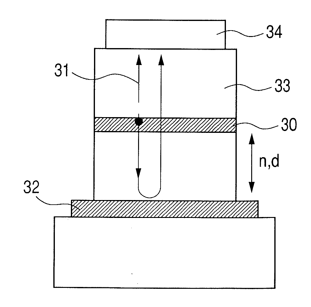
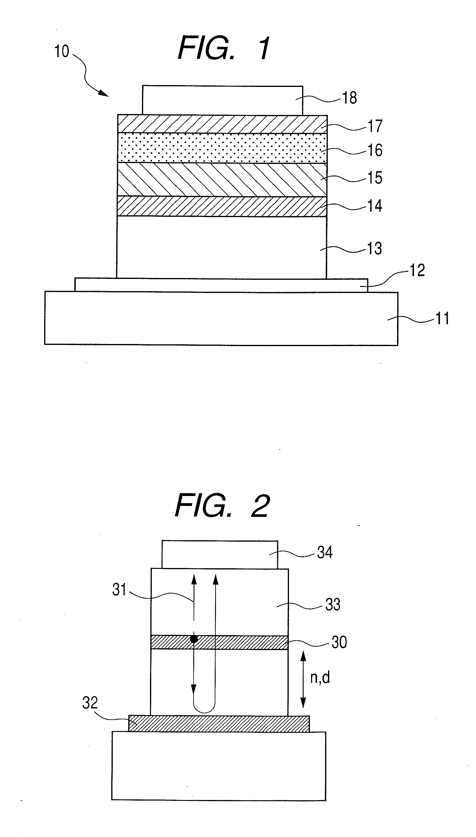
[0061]In this example, an organic light emitting apparatus was manufactured by preparing a substrate (100×100 dots) with an organic light emitting device having the same configuration as one described above as well as a reflective cathode 112. In this case, as the reflective cathode 112, an Al electrode was used. The configuration of an organic light emitting apparatus was schematically illustrated in FIG. 6. In addition, the thickness of each member of the organic light emitting device is shown in Table 1.

TABLE 1ComparativeExample 1example 1RGBRGBAnodeITO 80 nmITO 80 nmHole injection10 nm10 nmlayer (HIL)Hole transport30 nm30 nmlayer (HTL)Light emitting20 nm20 nm20 nm20 nm20 nm20 nmlayer (EML)Electron10 nm60 nm40 nm30 nmtransportlayer (ETL)Electron60 nm40 nm30 nm10 nminjectionlayer (EIL)CathodeAlAl

[006...

example 2

[0079]An example in which the interference peak of each color was under 3λ / 4 conditions was illustrated (not shown). In other words, an organic light emitting apparatus was manufactured, except for the following points: A reflection cathode was provided as a laminate structure of Al and 100 nm thick ITO. In addition, the electron injection layers for red, green, and blue had thicknesses of 120 nm, 70 nm, and 40 nm. Further, the thickness of each member included in the organic light emitting device is shown in Table 3.

TABLE 3ComparativeExample 2example 2RGBRGBAnodeITO 80 nmITO 80 nmHole injection10 nm10 nmlayer (HIL)Hole transport30 nm30 nmlayer (HTL)Light emitting 20 nm20 nm20 nm 20 nm20 nm20 nmlayer (EML)Electron10 nm120 nm70 nm40 nmtransportlayer (ETL)Electron120 nm70 nm40 nm10 nminjectionlayer (EIL)CathodeITO 100 nmITO 100 nmAlAl

[0080]The light emitting region in the light emitting layer, the refractive index, and the like are considered in a manner similar to those of Example 1....


PUM


Abstract

An organic light emitting apparatus comprising a substrate and a plurality of organic light emitting devices having different emission colors to each other formed on the substrate, each of the plurality of organic light emitting devices including a cathode, an electron injection layer which is in contact with the cathode, organic compound layers including a light emitting layer, and an optically-transparent anode, the electron injection layer including an organic compound and at least one of an alkali metal, an alkaline earth metal, an alkali metal compound, and an alkaline earth metal compound. The electron injection layer has a thickness adjusted for each of the different emission colors so that each of the plurality of organic light emitting devices having the different emission colors enhances light emitted from the light emitting layer.

Description

BACKGROUND OF THE INVENTION[0001]1. Field of the Invention[0002]The present invention relates to a top-emission type organic light emitting apparatus that includes a plurality of organic light emitting devices (organic EL devices) with two or more emission colors.[0003]2. Description of the Related Art[0004]In recent years, attentions have been paid to self-emitting devices for flat panels. The self-emitting devices include plasma-emission display devices, field emission devices, and electroluminescence (EL) devices.[0005]Of those, in particular, the organic light emitting devices have been energetically studied and developed. An area-color type organic light emitting apparatus, such as one with a single color of green or that with further added blue, red, or any of other colors, has been commercialized. Currently, development of a full-color type has been actively conducted.[0006]The organic compound layer of the organic light emitting apparatus, through which emitted light passes,...

Claims


Application Information

Patent Timeline
Patent Type & Authority Applications(United States)
IPC IPC(8): H01L51/52
CPCH01L51/5265H10K59/35H10K50/852
Inventor MIURA, SEISHIITO, NAOYUKIMATSUDA, YOJIRO
Owner CANON KK
Why Eureka
Try Eureka