PROCESS FOR FABRICATION OF FINFETs

Active Publication Date: 2008-05-15
GLOBALFOUNDRIES US INC
View PDF6 Cites 21 Cited by
  • Summary
  • Abstract
  • Description
  • Claims
  • Application Information

AI Technical Summary

Benefits of technology

[0025]The inventive structure provides improved gate to source/drain control since a portion of the gate dielectric

Problems solved by technology

Over the past twenty-five years or so, the primary challenge of very large scale integration (VLSI) has been the integration of an ever-increasing number of metal oxide semiconductor field effect transistor (MOSFET) devices with high yield

Method used


Image

  • PROCESS FOR FABRICATION OF FINFETs
  • PROCESS FOR FABRICATION OF FINFETs
  • PROCESS FOR FABRICATION OF FINFETs

Examples


Embodiment Construction

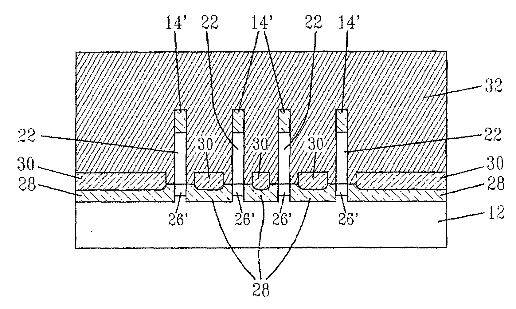
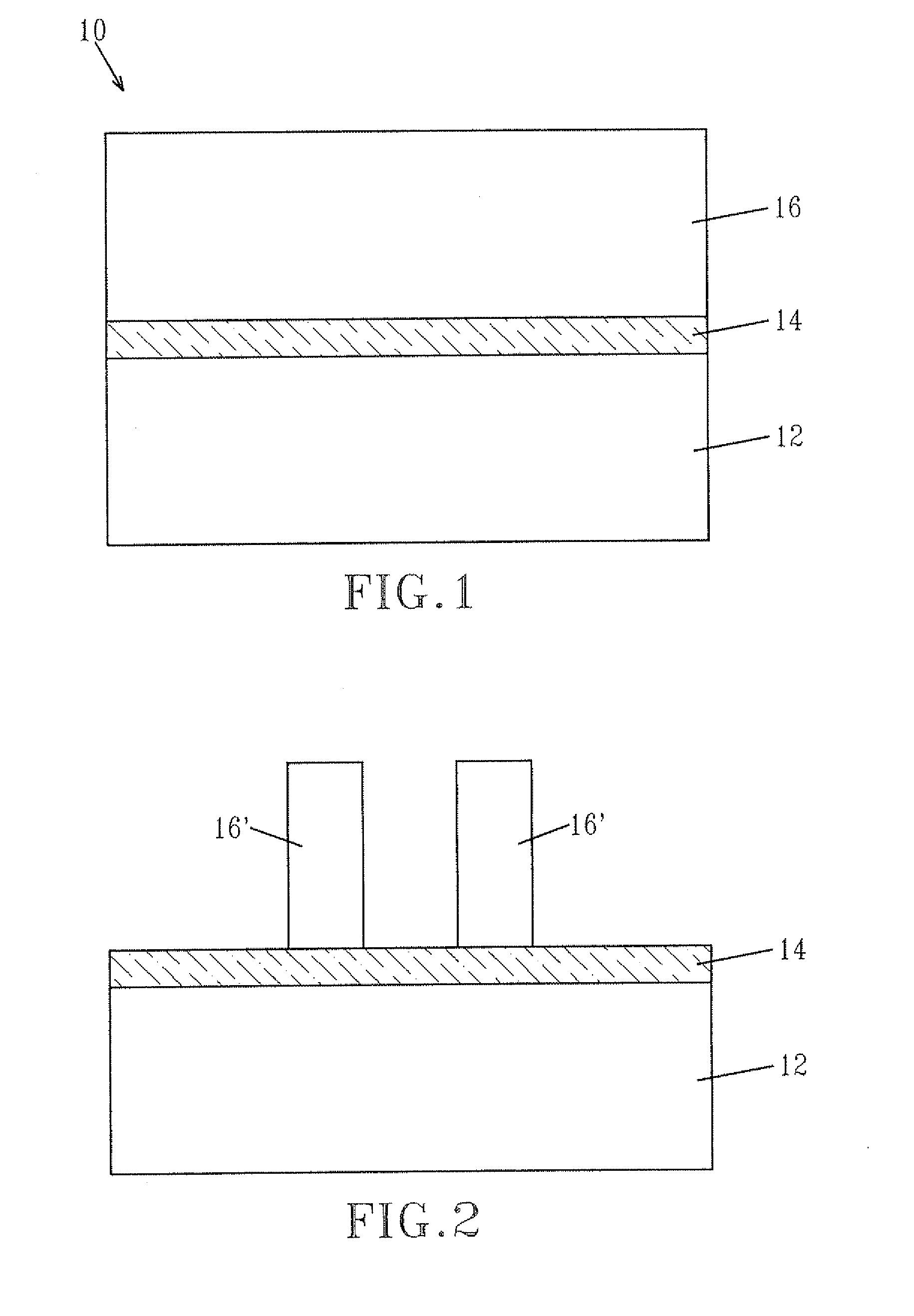
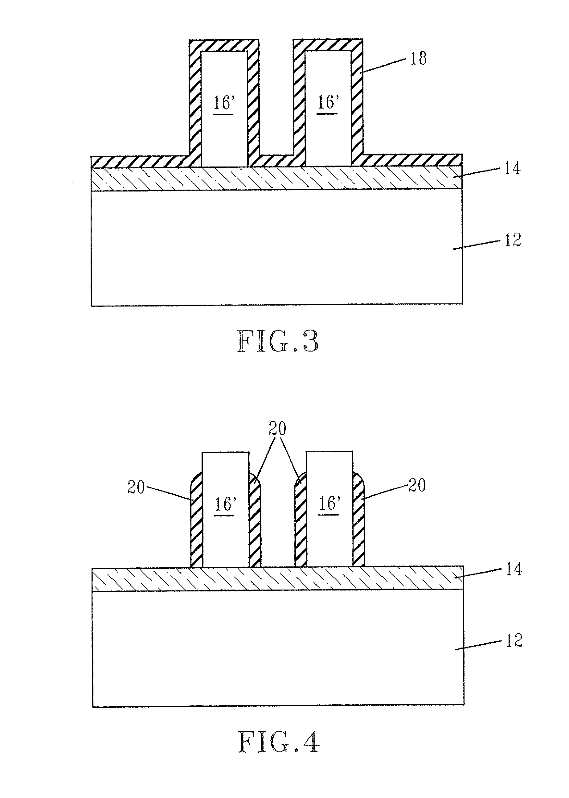
[0027]The present invention, which provides a method of fabricating FinFETs utilizing a single etching process which results in improved gate width control, will now be described in greater detail by referring to the following discussion and drawings that accompany the present application. It is noted that the drawings of the present application are provided for illustrative purposes and, as such, they are not drawn to scale.

[0028]In the following description, numerous specific details are set forth, such as particular structures, components, materials, dimensions, processing steps and techniques, in order to provide a thorough understanding of the present invention. However, it will be appreciated by one of ordinary skill in the art that the invention may be practiced with viable alternative process options without these specific details. In other instances, well-known structures or processing steps have not been described in detail in order to avoid obscuring the invention.

[0029]I...


PUM


Abstract

A method of fabricating a plurality of FinFETs on a semiconductor substrate in which the gate width of each individual FinFET is defined utilizing only a single etching process, instead of two or more, is provided. The inventive method results in improved gate width control and less variation of the gate width of each individual gate across the entire surface of the substrate. The inventive method achieves the above by utilizing a modified sidewall image transfer (SIT) process in which an insulating spacer that is later replaced by a gate conductor is employed and a high-density bottom up oxide fill is used to isolate the gate from the substrate.

Description

FIELD OF THE INVENTION[0001]The present invention relates to semiconductor device fabrication, and more particularly to a method of forming a plurality of FinFETs in which the gate width of each of the FinFETs is defined utilizing a single etching process that results in improved gate width control.BACKGROUND OF THE INVENTION[0002]Over the past twenty-five years or so, the primary challenge of very large scale integration (VLSI) has been the integration of an ever-increasing number of metal oxide semiconductor field effect transistor (MOSFET) devices with high yield and reliability. This was achieved mainly in the prior art by scaling down the MOSFET channel length without excessive short-channel effects. As is known to those skilled in the art, short-channel effects are the decrease of threshold voltage Vt in short-channel devices due to two-dimensional electrostatic charge sharing between the gate and the source / drain diffusion regions.[0003]To scale down MOSFET channel lengths wi...

Claims


Application Information

Patent Timeline
IPC IPC(8): H01L29/78H01L21/336
CPCH01L29/7851H01L29/66795
Inventor BEINTNER, JOCHENBRONNER, GARY B.DIVAKARUNI, RAMACHANDRALI, YUJUN
Owner GLOBALFOUNDRIES US INC
Why Eureka
Try Eureka