Overmolded electronic module with an integrated electromagnetic shield using SMT shield wall components

a technology of electromagnetic shielding and electronic modules, applied in the direction of final product manufacturing, sustainable manufacturing/processing, semiconductor/solid-state device details, etc., can solve the problems of adversely affecting the circuitry of the electronic module, exceeding the regulatory limit, and affecting other electronic devices, etc., to achieve mechanical stability, withstand subsequent overmolding processes, and facilitate manufacturing

Inactive Publication Date: 2008-05-15
SKYWORKS SOLUTIONS INC
View PDF8 Cites 40 Cited by
  • Summary
  • Abstract
  • Description
  • Claims
  • Application Information

AI Technical Summary

Benefits of technology

[0010]Multiple module circuit boards can be arranged in an array on a circuit board panel or strip with a space between the module circuit boards that is used as a saw street when the module circuit boards go through a singulation process. The design of the SMT shield wall components allows them to be placed between module circuit boards in the saw street such that one SMT shield wall component can provide a first shield wall section for a given module circuit board and a second shield wall section for

Problems solved by technology

Such electromagnetic signals can radiate through the non-conductive packaging material of the electronic module and affect other electronic devices (e.g., cause interference), exceed regulatory limits, and/or be subject to interception.
Also, externally present electromagnetic energy of either natural or artificial origin may penetrate non-conductive packaging material of an electronic module to adversely affect the circ

Method used


Image

  • Overmolded electronic module with an integrated electromagnetic shield using SMT shield wall components
  • Overmolded electronic module with an integrated electromagnetic shield using SMT shield wall components
  • Overmolded electronic module with an integrated electromagnetic shield using SMT shield wall components

Examples


Embodiment Construction

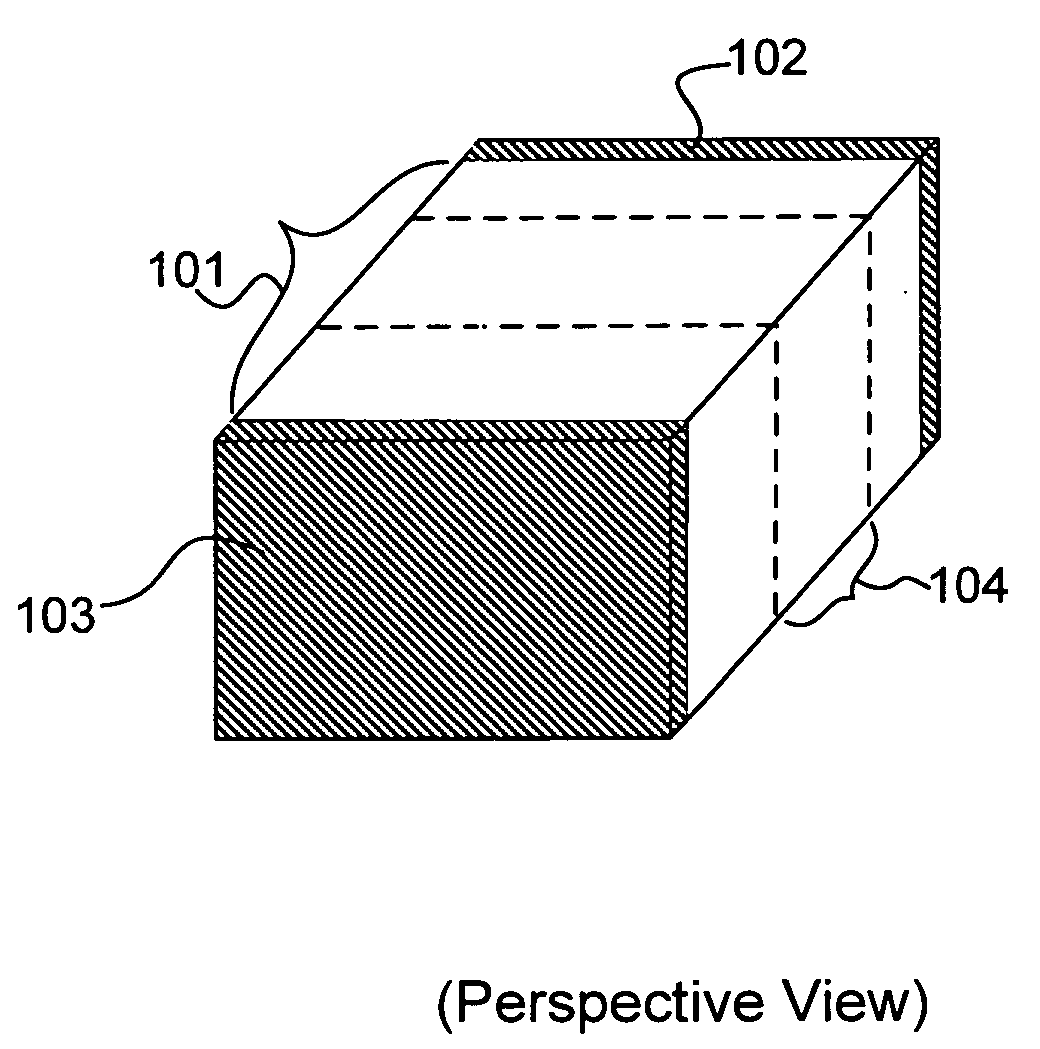
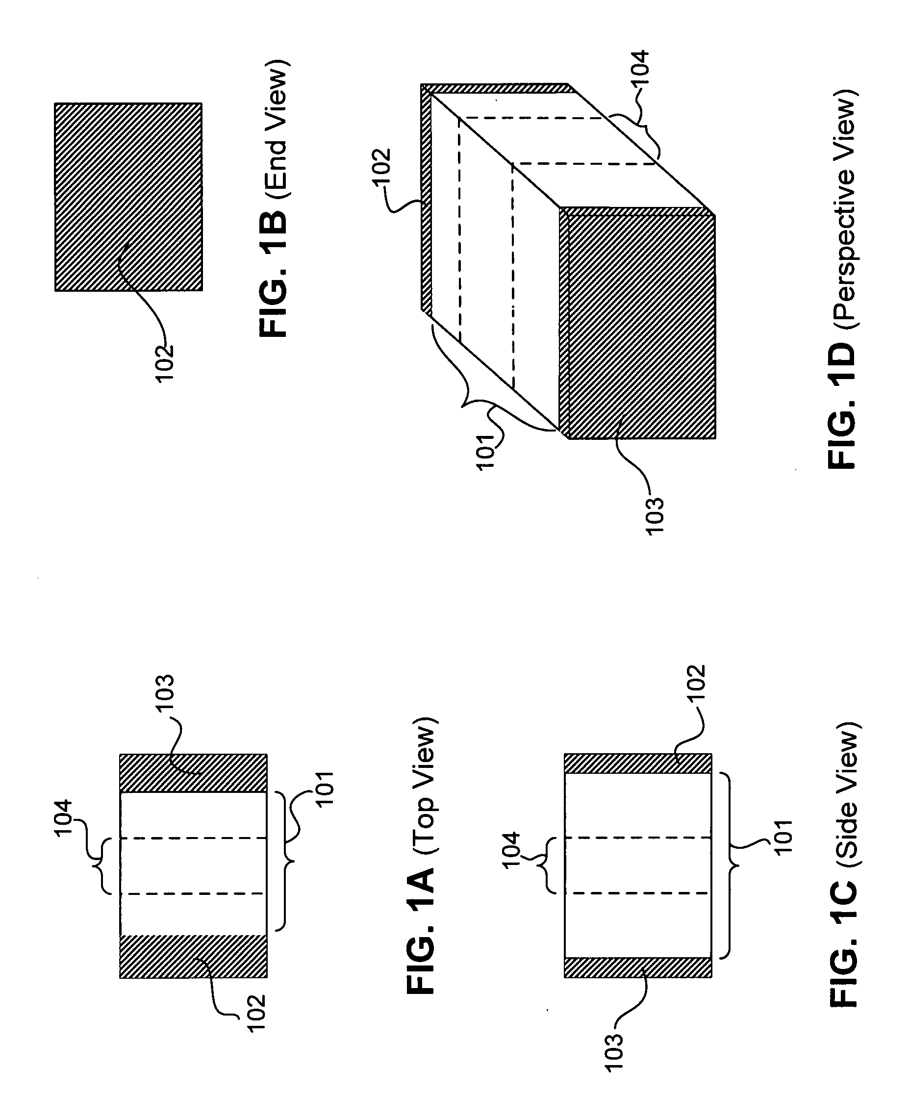
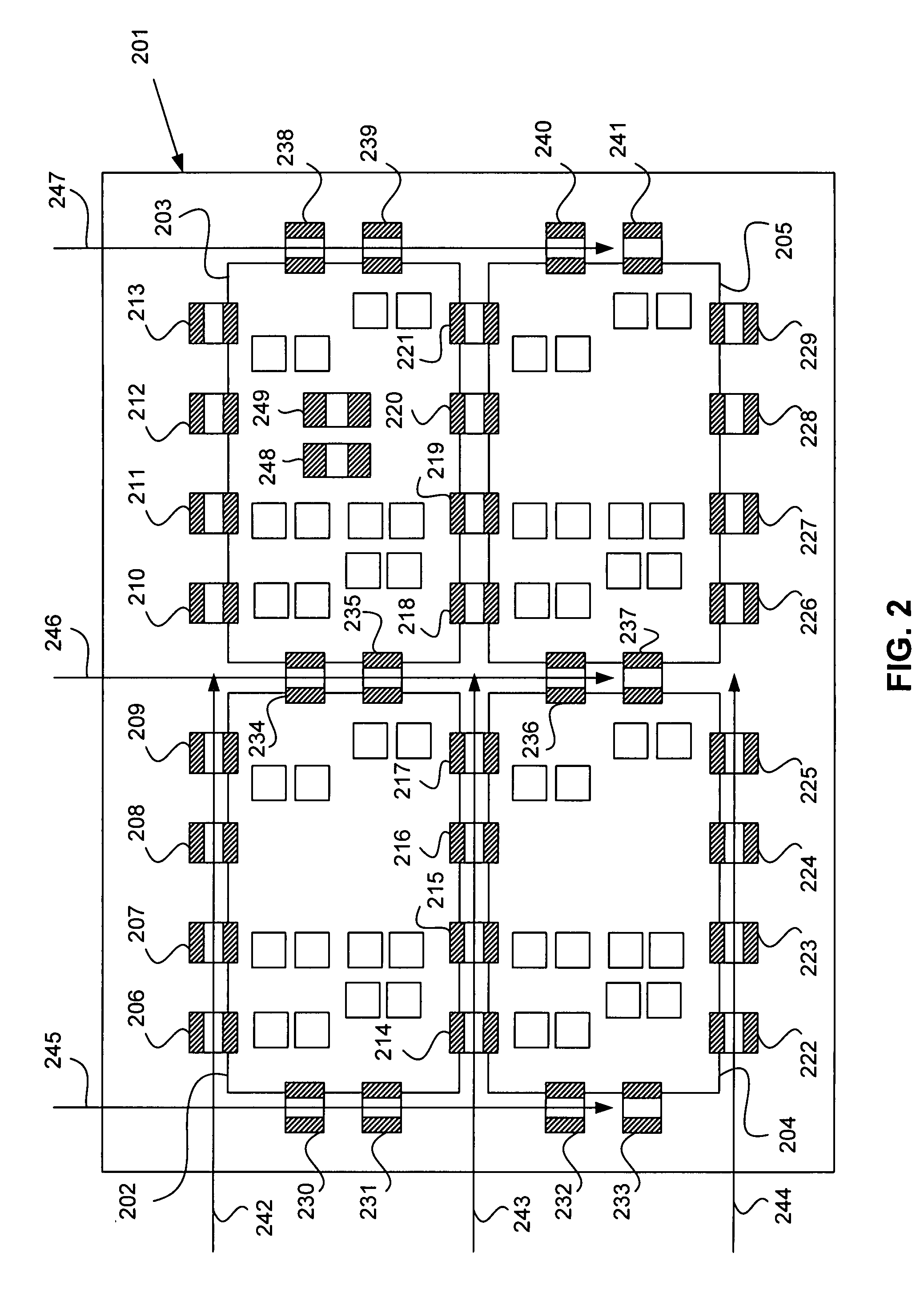
[0018]The present invention is directed to a method and apparatus for an electronic module with an overmolded electromagnetic shield using SMT shield wall components. The following description contains specific information pertaining to the implementation of the present invention. One skilled in the art will recognize that the present invention may be implemented in a manner different from that specifically discussed in the present application. Moreover, some of the specific details of the invention are not discussed in order not to obscure the invention. The specific details not described in the present application are within the knowledge of a person of ordinary skill in the art.

[0019]The drawings in the present application and their accompanying detailed description merely describe exemplary embodiments of the invention. To maintain brevity, other embodiments of the invention which use the principles of the present invention are not specifically described in the present applicati...


PUM

PropertyMeasurementUnit
Electrical conductoraaaaaaaaaa
Stabilityaaaaaaaaaa
Mechanical stabilityaaaaaaaaaa

Abstract

An electronic module with an integrated electromagnetic shield using surface mount shield wall components has been disclosed. Each surface mount shield wall component provides side shielding of circuitry within the overmolded electronic module and provides an exposed conductive shield wall section to which a top conductive shield can be applied. By including the shield structure as part of the overmolded electronic module, the need for a separate shield and separate process steps for installing the separate shield can be eliminated. Each surface mount shield wall component comprises a non-conductive portion that provides stability during a reflow soldering process, but at least a sacrificial portion of the non-conductive portion can be removed to reduce the amount of area occupied by the overmoldable shield structure.

Description

[0001]This application is a continuation in part of, and claims benefit of the filing date of, and hereby incorporates fully by reference, the pending parent application entitled “Overmolded Semiconductor Package with an Integrated EMI and RFI Shield” Ser. No. 10 / 793,618, filed Mar. 4, 2004, and assigned to the assignee of the present application.BACKGROUND OF THE INVENTION[0002]1. Field of the Invention[0003]The invention relates generally to electronic device manufacturing and more particularly to techniques for providing shielding for electronic components.[0004]2. Related Art[0005]Portable electronic devices such as cell phones typically utilize electronic modules to provide a high level of functionality in a small package. The electronic module can include, for example, any combination of one or more integrated circuits and one or more passive devices such as resistors, capacitors, and inductors mounted on a module circuit board. The components of the electronic module can be e...

Claims


Application Information

Patent Timeline
IPC IPC(8): H05K7/00H01L23/31H01L23/552
CPCH01L23/3121Y10T29/49144H01L24/97H01L2924/01029H01L2924/14H01L2924/19041H01L2924/19042H01L2924/19043H01L2924/3025H05K3/0052H05K3/3405H05K3/3442H05K2201/10204H05K2201/10371H05K2201/10636H01L2924/01006H01L2924/01033H01L2924/014H01L2224/48227H01L2224/97H01L23/552Y10T29/4913H05K9/0088H01L2224/85H01L2924/181Y02P70/50H01L2924/00
Inventor THOMPSON, PHILIP H.POTTEBAUM, LARRY D.
Owner SKYWORKS SOLUTIONS INC
Why Eureka
Try Eureka