Semiconductor device and method of forming the same

Active Publication Date: 2008-05-22
LONGITUDE LICENSING LTD
View PDF1 Cites 26 Cited by
  • Summary
  • Abstract
  • Description
  • Claims
  • Application Information

AI Technical Summary

Benefits of technology

[0019]It is an additional object of the present invention to provide a method of forming a semiconductor device free from the above-described problems or disadvantages.
[0020]It is another object of the present invention to provide a method of forming a semiconductor device that can suppress short channel effects.
[0021]It is still another object of the present invention

Problems solved by technology

As a result, the impurity concentration of the source and drain diffusion re

Method used


Image

  • Semiconductor device and method of forming the same
  • Semiconductor device and method of forming the same
  • Semiconductor device and method of forming the same

Examples


Embodiment Construction

[0058]Selected embodiments of the present invention will now be described with reference to the drawings. It will be apparent to those skilled in the art from this disclosure that the following descriptions of the embodiments of the present invention are provided for illustration only and not for the purpose of limiting the invention as defined by the appended claims and their equivalents.

[0059]In the following embodiment, a semiconductor device is applied to a DRAM.

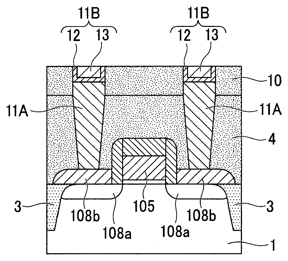
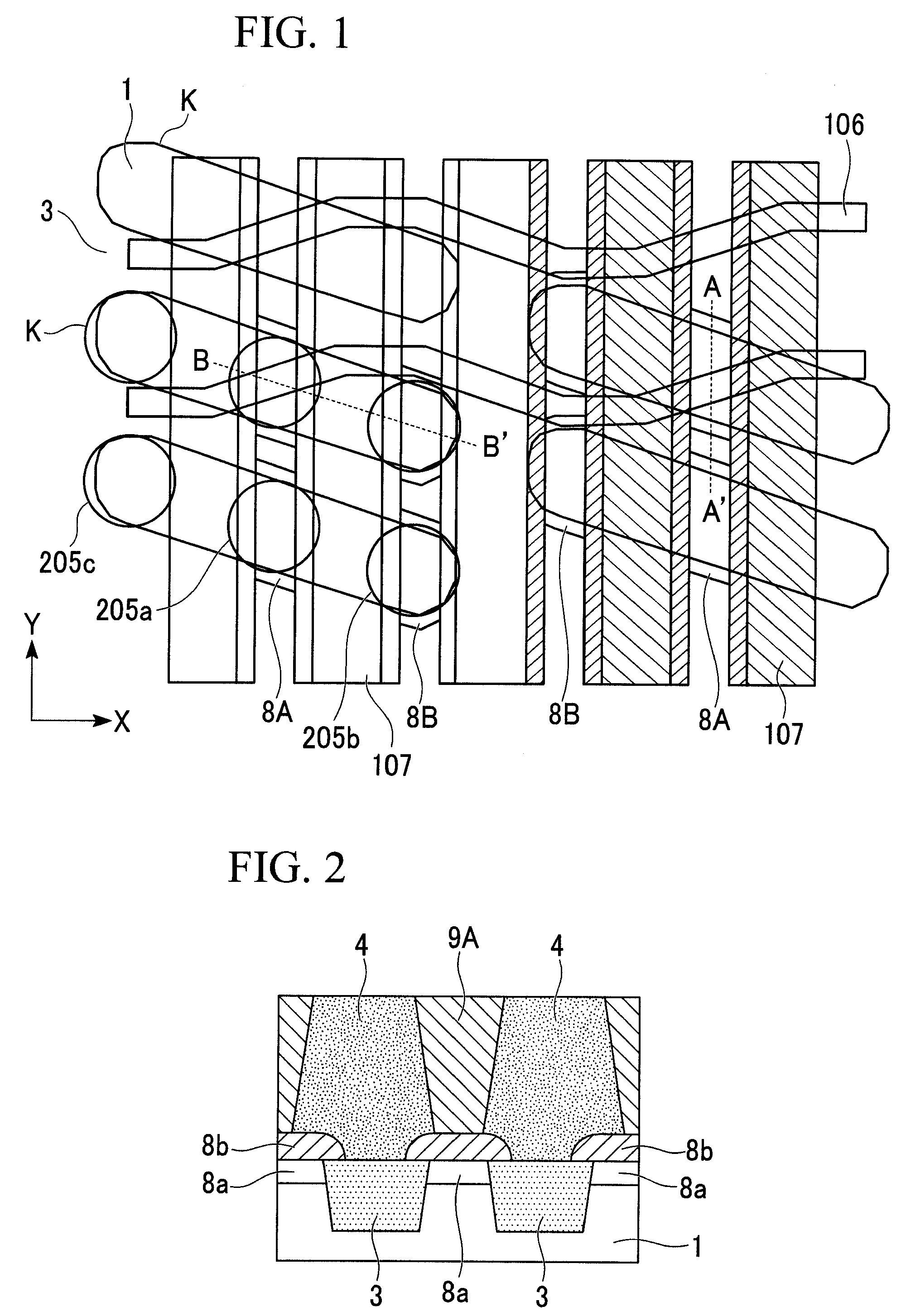
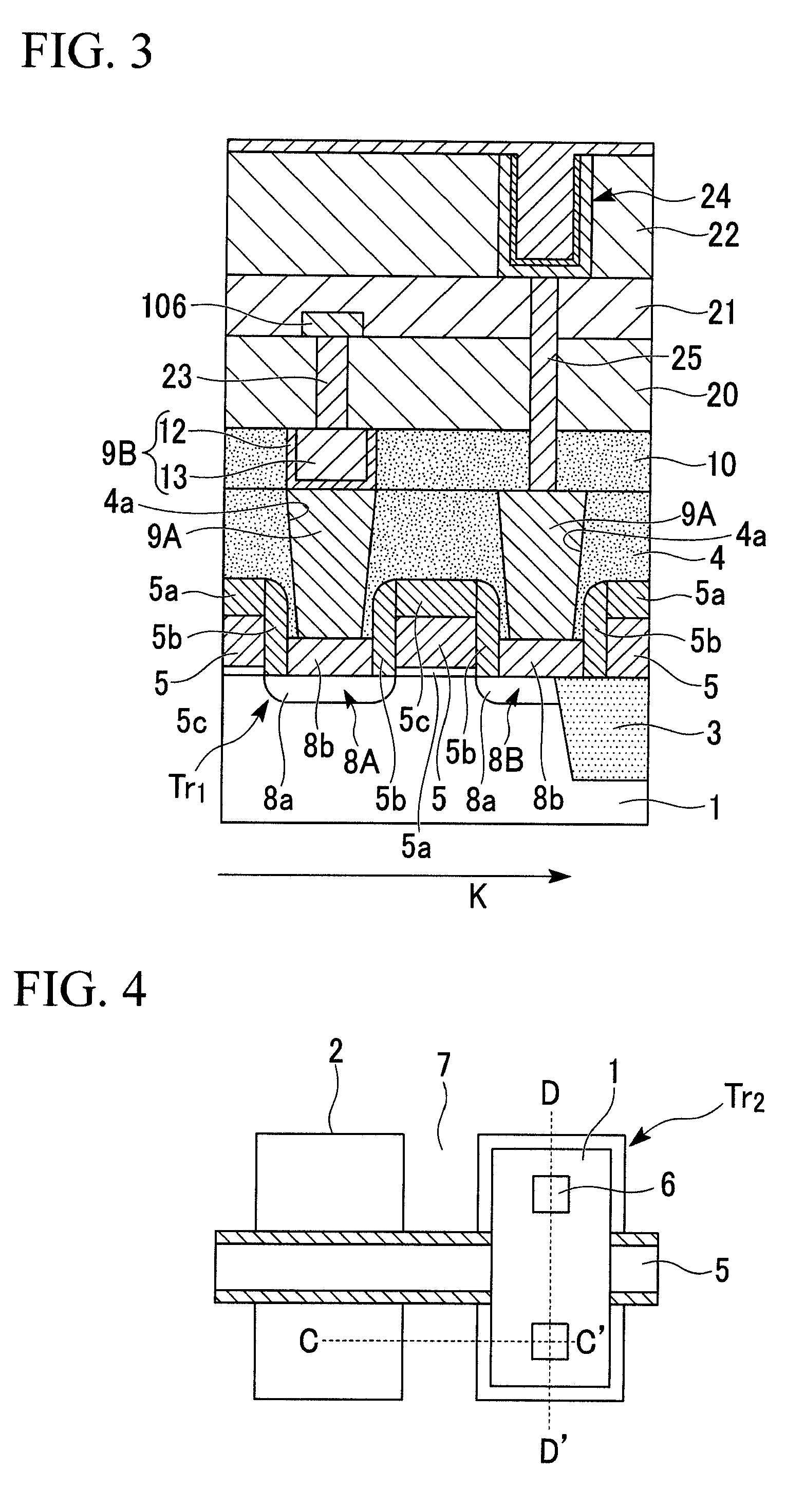
[0060]FIG. 1 is a fragmentary plan view illustrating an array of memory cells of a semiconductor device in accordance with a first embodiment of the present invention. FIG. 2 is a fragmentary cross sectional elevation view illustrating the semiconductor device, taken along an A-A′ line of FIG. 1. FIG. 3 is a fragmentary cross sectional elevation view illustrating a memory cell structure of the semiconductor device, taken along a B-B′ line of FIG. 1. FIG. 4 is a fragmentary plan view illustrating a part of peripheral circ...


PUM


Abstract

A semiconductor device includes a semiconductor substrate, source and drain regions on the semiconductor substrate, and contact plugs connected to the source and drain regions. The contact plugs includes first impurity-diffused epitaxial layers that contact with the source and drain regions.

Description

BACKGROUND OF THE INVENTION[0001]1. Field of the Invention[0002]The present invention generally relates to a semiconductor device and a method of forming the same.[0003]Priority is claimed on Japanese Patent Application No. 2006-313179, filed Nov. 20, 2006, the content of which is incorporated herein by reference.[0004]2. Description of the Related Art[0005]All patents, patent applications, patent publications, scientific articles, and the like, which will hereinafter be cited or identified in the present application, will hereby be incorporated by reference in their entirety in order to describe more fully the state of the art to which the present invention pertains.[0006]In recent years, computers or electric devices include one or more large scale integrated circuits, hereinafter referred to as LSI, in which a large number of MOS transistors and resistances may typically be integrated on a single chip. Dynamic random access memories (DRAMs) include LSIs. The DRAM needs shrinkage ...

Claims


Application Information

Patent Timeline
IPC IPC(8): H01L21/336H01L29/40
CPCH01L21/28525H01L21/76879H01L21/76886H01L23/485H01L27/10855H01L27/10888H01L2924/0002H01L27/10894H01L29/41783H01L29/66575H01L2924/00H10B12/485H10B12/09H10B12/0335
Inventor YUKI, KAZUYOSHI
Owner LONGITUDE LICENSING LTD
Why Eureka
Try Eureka