Method for forming field effect transistor and field effect transistor

A field effect transistor and gate technology, applied in the field of semiconductor manufacturing process design, can solve problems such as poor performance of FinFET

Pending Publication Date: 2020-09-01
SEMICON MFG INT (SHANGHAI) CORP +1
View PDF10 Cites 0 Cited by
  • Summary
  • Abstract
  • Description
  • Claims
  • Application Information

AI Technical Summary

Problems solved by technology

[0007] The purpose of the present invention is to solve t

Method used


Image

  • Method for forming field effect transistor and field effect transistor
  • Method for forming field effect transistor and field effect transistor
  • Method for forming field effect transistor and field effect transistor

Examples


Embodiment 1

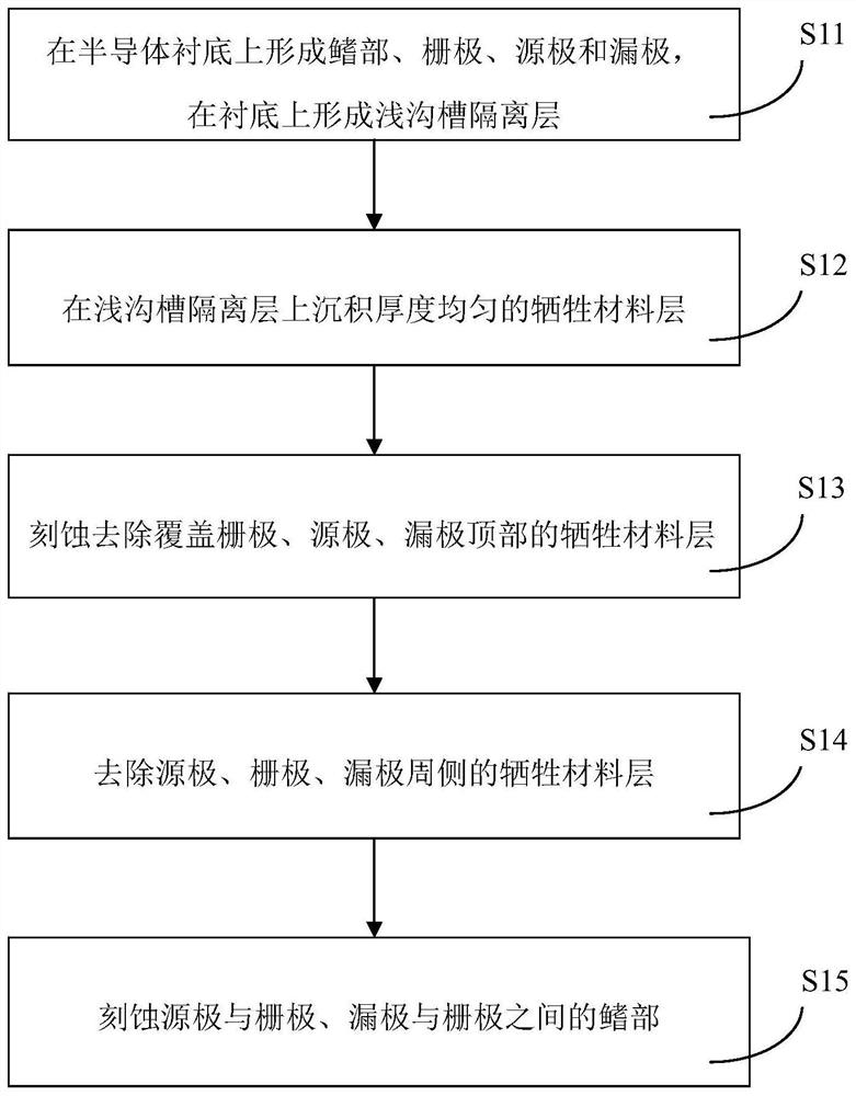
[0039] In order to solve the problem of poor performance of FinFET in the prior art, a method for forming a field effect transistor is proposed. Specifically, see figure 1 , the method for forming the field effect transistor provided in this embodiment includes:

[0040] Step S11: forming a fin, a gate, a source and a drain on the semiconductor substrate, and forming a shallow trench isolation layer on the substrate. More specifically, a semiconductor substrate is provided, and fins are first formed on the semiconductor substrate, then a gate, a source and a drain are formed, and finally a shallow trench isolation layer is formed on the substrate. The substrate is set at the bottom of the field effect transistor and is made of semiconductor material. More specifically, the material of the substrate may be, but not limited to, a sapphire substrate, a silicon carbide substrate, or a silicon substrate. This embodiment uses a silicon substrate.

[0041] Further, the fin is form...

Embodiment 2

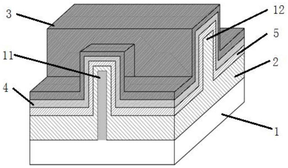
[0060] Based on the method for forming a field effect transistor provided in Embodiment 1, this embodiment provides a method for forming a field effect transistor in which the hard mask layer is a gate mask. Specifically, see Figure 3a-Figure 3e , the steps of the process of forming the FinFET using the gate mask 51 as its hard mask layer 5 may specifically be:

[0061] For the first step, see Figure 3a , providing a semiconductor substrate 1 , forming a fin 11 , a gate 12 , a source 13 and a drain 14 on the semiconductor substrate, and forming a shallow trench isolation layer 2 on the substrate 1 .

[0062] In the second step, see Figure 3b , depositing a sacrificial material layer 3 with a uniform thickness on the shallow trench isolation layer 2 .

[0063] Step three, see Figure 3c , etch and remove the sacrificial material layer 2 covering the tops of the gate 12 , the source 13 and the drain 14 .

[0064] For step four, see Figure 3d , remove the sacrificial ma...

Embodiment 3

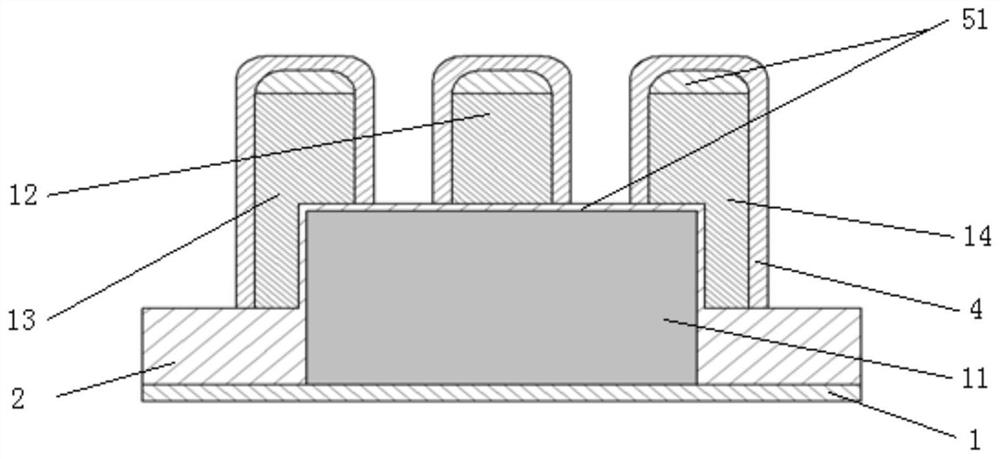
[0073] Based on the method for forming a field effect transistor provided in Embodiment 1, this embodiment provides a method for forming a field effect transistor in which the hard mask layer is a well mask. Specifically, see Figure 4a-Figure 4f , the steps of the process of forming the FinFET using the well mask 52 as its hard mask layer 5 may specifically be:

[0074] For the first step, see Figure 4a , providing a semiconductor substrate 1 , forming a fin 11 , a gate 12 , a source 3 and a drain 14 on the semiconductor substrate 1 , and forming a shallow trench isolation layer 2 on the substrate 1 .

[0075] In the second step, see Figure 4b , depositing a sacrificial material layer 3 with a uniform thickness on the shallow trench isolation layer 2 .

[0076] Step three, see Figure 4c , etching and removing the sacrificial material layer 3 covering the tops of the gate 12 , the source 13 and the drain 14 .

[0077] For step four, see Figure 4d , etch the sacrifici...


PUM


Abstract

The invention discloses a method for forming a field effect transistor. The method comprises the following steps of providing a semiconductor substrate, forming a fin part, a grid electrode, a sourceelectrode and a drain electrode on the semiconductor substrate, and forming a shallow trench isolation layer on the substrate; depositing a sacrificial material layer with uniform thickness on the shallow trench isolation layer; etching to remove the sacrificial material layer covering the tops of the grid electrode, the source electrode and the drain electrode; removing the sacrificial material layers at the peripheral sides of the source electrode, the grid electrode and the drain electrode; and etching the fin part between the source electrode and the grid electrode, and etching the fin part between the drain electrode and the grid electrode to a position lower than the top of the shallow trench isolation layer or a position flush with the top of the shallow trench isolation layer. Themethod for forming the field effect transistor provided by the invention is simple and convenient to operate, and the grooves formed after the fin parts between the grid electrode and the source electrode and between the grid electrode and the drain electrode are respectively etched can be effectively enlarged, so that the size of the epitaxial layer arranged in the grooves can be increased, and the short-channel effect is further reduced. The invention also provides the field effect transistor which is formed by the method and has more stable performance.

Description

technical field [0001] The invention relates to the field of semiconductor manufacturing process design, in particular to a method for forming a field effect transistor and a field effect transistor formed according to the method. Background technique [0002] In order to keep up with Morgan's law, the size of integrated circuit devices is continuously reduced to meet the requirements of high device density, high performance, and low cost. For example, diodes, triodes, etc., while the size of the device is reduced, the distance between the source and drain of the device is also shortened. As a result, the control ability of the gate to the channel is deteriorated, and the short channel effect is easily generated. [0003] In order to suppress the short-channel effect, three-dimensional field effect transistors, such as fin field effect transistors (FinFETs), gradually occupy the stage. Compared with the planar field effect transistor, the gate of the FinFET has a stronger ...

Claims


Application Information

Patent Timeline
IPC IPC(8): H01L21/336H01L29/06H01L29/10H01L29/78
CPCH01L29/66795H01L29/785H01L29/1033H01L29/0684
Inventor 王楠
Owner SEMICON MFG INT (SHANGHAI) CORP
Why Eureka
Try Eureka