

Semiconductor device and manufacturing method thereof
- Summary
- Abstract
- Description
- Claims
- Application Information
AI Technical Summary
Benefits of technology
Problems solved by technology
Method used
Image

Examples
Embodiment Construction
[0053]The invention will be now described herein with reference to illustrative embodiments. Those skilled in the art will recognize that many alternative embodiments can be accomplished using the teachings of the present invention and that the invention is not limited to the embodiments illustrated for explanatory purposes.
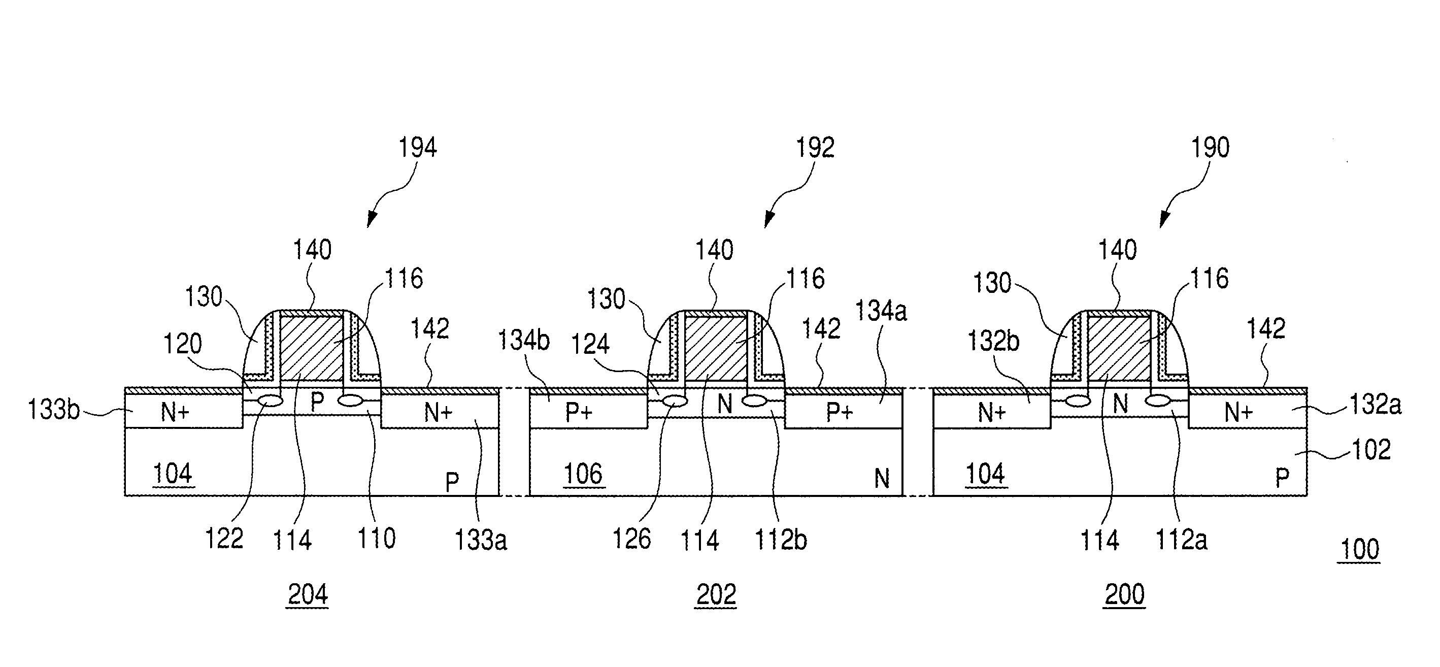
[0054]In FIGS. 12(a), (b), and (c) a semiconductor device 10 uses an NMOS transistor as an anti-fuse, with FIG. 12(a) being before breakdown of a gate dielectric film and FIGS. 12(b) and 12(c) being after breakdown of the gate dielectric film.
[0055]As illustrated in FIG. 12(a), the semiconductor device 10 has a p well 12, source / drain regions 14 formed in the surface of the p well 12, and a gate 19 formed over the p well 12. The gate 19 has a gate dielectric film 20, a gate electrode 22, a silicide layer 24 formed over the surface of the gate electrode 22, and sidewalls 25 formed on both sides of the gate electrode 22. Silicide layer 15 is also formed in the surf...
PUM
 Abstract
Description
Claims
Application Information