Contact tip structure for microelectronic interconnection elements and methods of making same

a technology of interconnection elements and contact tips, which is applied in the direction of individual semiconductor device testing, instruments, solid-state devices, etc., can solve the problems of increasing the difficulty of grinding the tip, increasing the difficulty of controlling or establishing the desired shape at the contact end, and requiring frequent rework. to achieve the effect of precise uniformity

Inactive Publication Date: 2008-05-22
FORMFACTOR INC
View PDF2 Cites 7 Cited by
  • Summary
  • Abstract
  • Description
  • Claims
  • Application Information

AI Technical Summary

Benefits of technology

[0020] It is an object of the present invention to provide an improved technique for fabricating interconnection elements, particularly for use in interconnecting microelectronic components.
[0029] Generally, the invention facilitates the construction of electrical contact structures by joining a plurality of contact tip structures having a relatively precise positional relationship with one another to a corresponding plurality of interconnection elements which may be disposed in relatively rough (coarse) relationship with one another. Preferably, each contact tip structure has a topological contact feature portion on its body portion which is disposed in relatively precise relationship to other ones of the topological contact features, so that the body portions of the tip structures need not be located so precisely with respect to one another. These topological contact features are readily formed with great positional precision by etching the sacrificial substrate upon which the contact tip structure is pre-fabricated so that they take the form (shape) of pyramids, truncated pyramids, and the like, using conventional semiconductor fabrication processes including micromachining.
[0033] An important feature of the present invention is that a plurality of contact tip structures are readily fabricated on a sacrificial substrate to extremely precise tolerances, for example, by using known semiconductor fabrication processes such as masking, lithography and deposition to control their size and spacing.
[0041] The present invention provides a technique for fabricating relatively ‘perfect’ (extremely uniform and reproducible to close tolerances) contact tip structures and ‘marrying’ them to relatively ‘imperfect’ interconnection elements. Due to the constraints associated with making interconnection elements, certain tradeoffs are often required vis-a-vis the tip geometry and metallurgy, and overall spatial uniformity of the interconnection elements. And, if they can't be reworked, they must be replaced. The present invention solves this limitation by freeing up the tip metallurgy, geometry, and topology from that of the interconnection element to which it is joined, with lithographically precise uniformity.

Problems solved by technology

Problems with tungsten needles include difficulties in grinding their tips to have an appropriate shape, they don't last long, and they require frequent rework.
Returning to the example of tungsten needles as probe elements, the metallurgy of the contact end is evidently limited by the metallurgy (i.e., tungsten) of the interconnection element and, as these tungsten needles become smaller and smaller in diameter, it becomes commensurately more difficult to control or establish a desired shape at their contact ends.
Again, the technology required to manufacture such interconnection elements limits the design choices for the shape and metallurgy of the contact portions of such interconnection elements.

Method used


Image

  • Contact tip structure for microelectronic interconnection elements and methods of making same
  • Contact tip structure for microelectronic interconnection elements and methods of making same
  • Contact tip structure for microelectronic interconnection elements and methods of making same

Examples


example 1

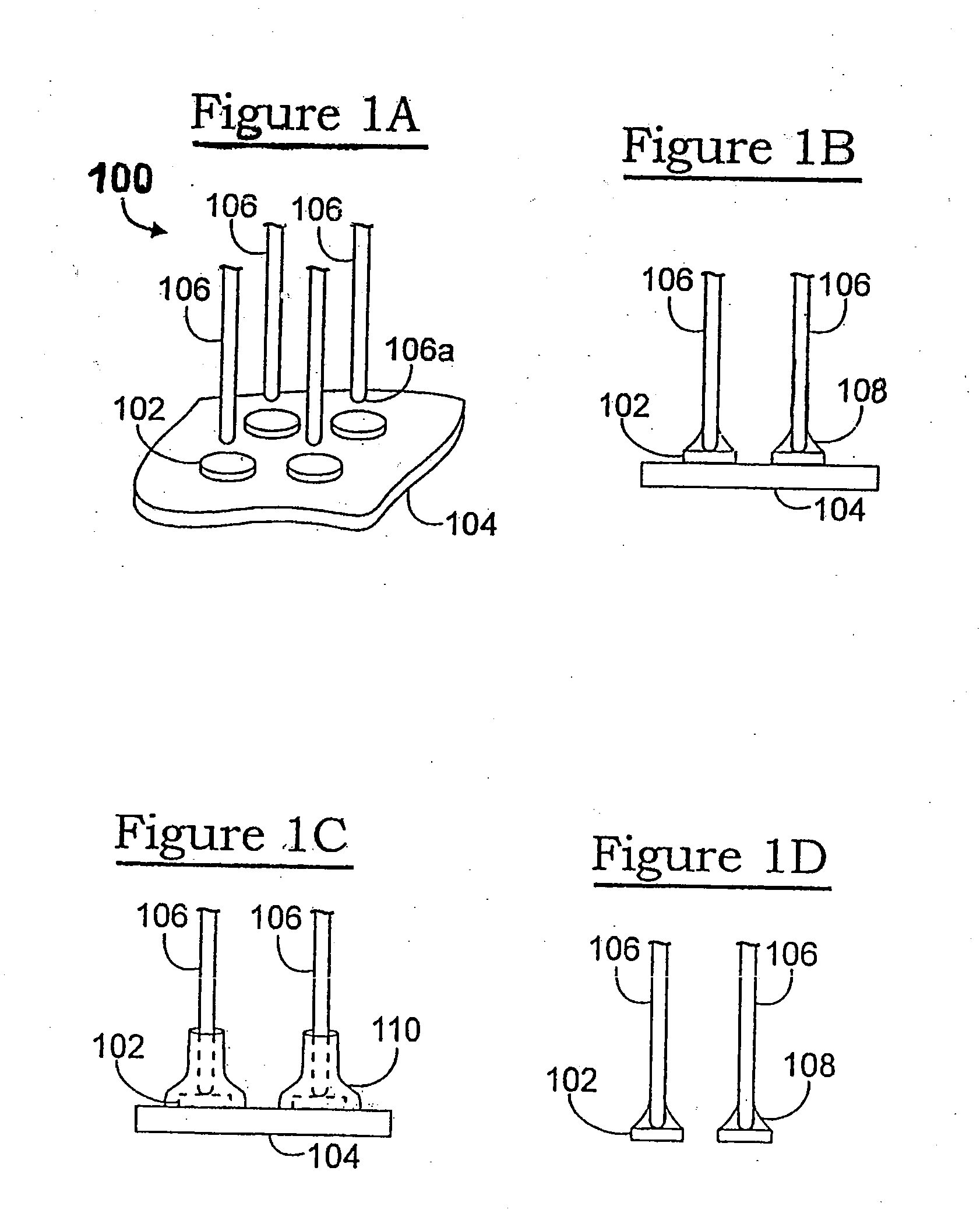
[0111] An example of a plurality of elongate interconnection elements which are not mounted by their ends to a substrate is the IBM™ Cobra™ probe which, as shown (stylized) in FIG. 3A, has a plurality (four of many shown) of elongate interconnection elements 302 extending generally parallel to each other between two rigid fixed planar structures 304 and 306, the two opposite ends of each interconnection element 302 being exposed through a respective one of the two rigid fixed planar structures for making a pressure connection between a terminal (not shown) of a one electronic component (not shown) and a terminal (not shown) of another electronic component (not shown). The illustration of FIG. 3A is schematic in nature, and is not intended to be a mechanical assembly drawing. The elongate interconnection elements 302 can be kinked, and generally function as buckling beams.

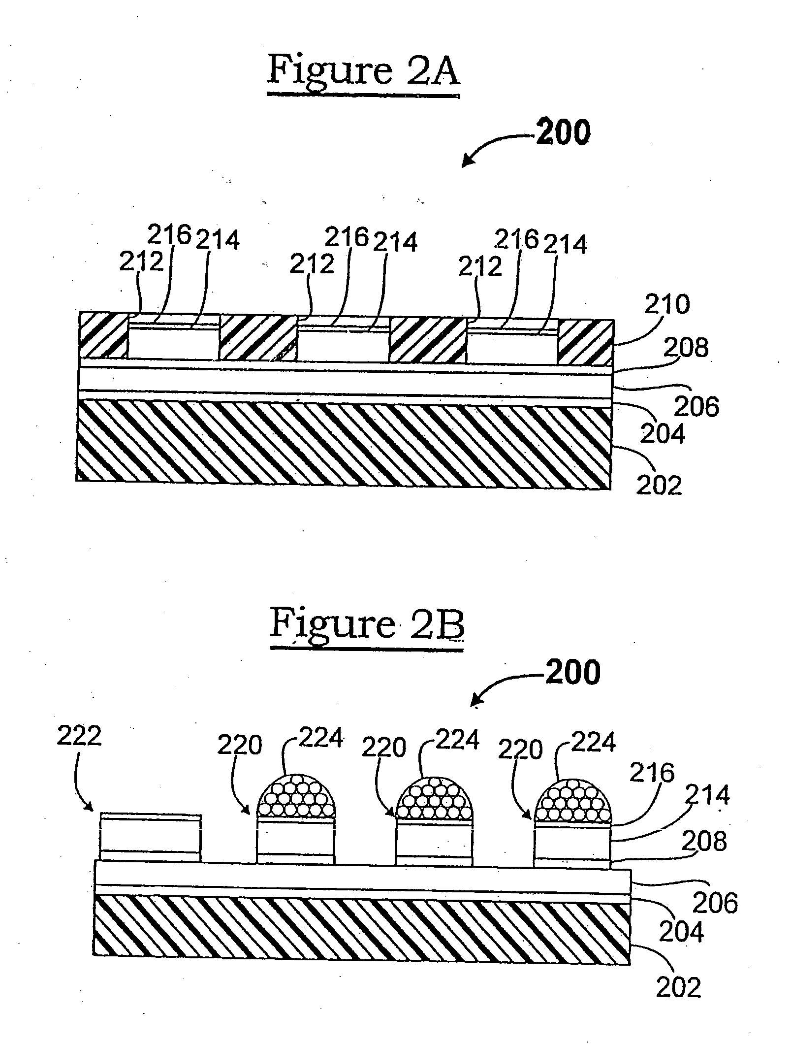
[0112] Prefabricated contact tip structures, for example the tip structures 220 shown in FIG. 2B hereinabove, ar...

example 2

[0115]FIG. 3B illustrates a one of a plurality of contact tip structures 220 joined (such as by brazing or plating, discussed hereinabove, not shown) to an end of an elongate tungsten needle 312 which is a typical element of a prior art probe card (not shown).

[0116] This illustrates, in an exemplary manner, an important advantage of the present invention. It is generally difficult to provide existing tungsten needles of probe cards with a desired tip shape, especially as the needles are getting smaller and smaller in size (e.g., having a diameter of 1 mil). By joining prefabricated contact tip structures (220) to the ends of tungsten needles (312), these problems may be avoided, thereby facilitating the use of ever smaller (e.g., in diameter) tungsten needles while providing contact surfaces (i.e., of the contact tip structures) which are larger (in diameter, or “footprint”) than the tungsten needles. The present invention also overcomes, for example, the difficulty in controlling ...

example 3

[0119] The interconnection elements to which the contact tip structures are joined will often be elongate, and may be inherently resilient, such as in the previous two examples. It is, however, within the scope of the present invention that the interconnection elements to which the contact tip structures are joined are neither elongate nor inherently resilient.

[0120]FIG. 3C illustrates a portion of a membrane probe of the type known in the prior art wherein a plurality (two of many shown) of non-resilient bump interconnection elements (contact bumps) 322 are resident on a surface of a flexible membrane 324. As illustrated, the contact tip structures of the present invention, for example the tip structures 220 are joined (such as by brazing or plating, discussed hereinabove, not shown) to the interconnection elements 322. For purposes of this discussion, the rounded bumps 322 are considered to have “tips” or “ends” at their apex (their top edge, as viewed).

[0121] The ability to joi...


PUM


Abstract

Contact tip structures are fabricated on sacrificial substrates for subsequent joining to interconnection elements including composite interconnection elements, monolithic interconnection elements, tungsten needles of probe cards, contact bumps of membrane probes, and the like. The spatial relationship between the tip structures can lithographically be defined to very close tolerances. The metallurgy of the tip structures is independent of that of the interconnection element to which they are attached, by brazing, plating or the like. The contact tip structures are readily provided with topological (small, precise, projecting, non-planar) contact features, such as in the form of truncated pyramids, to optimize electrical pressure connections subsequently being made to terminals of electronic components. Elongate contact tip structures, adapted in use to function as spring contact elements without the necessity of being joined to resilient contact elements are described. Generally, the invention is directed to making (pre-fabricating) relatively ‘perfect’ contact tip structures (“tips”) and joining them to relatively ‘imperfect’ interconnection elements to improve the overall capabilities of resulting “tipped” interconnection elements.

Description

CROSS-REFERENCE TO RELATED APPLICATIONS [0001] This patent application is a continuation-in-part of commonly-owned, copending U.S. patent application Ser. No. 08 / 452,255 (hereinafter “PARENT CASE”) filed 26 May 1995 and its counterpart PCT patent application number PCT / US95 / 14909 filed 13 Nov. 1995, both of which are continuations-in-part of commonly-owned, copending U.S. patent application Ser. No. 08 / 340,144 filed 15 Nov. 1994 and its counterpart PCT patent application number PCT / US94 / 13373 filed 16 Nov. 1994, both of which are continuations-in-part of commonly-owned, copending U.S. patent application Ser. No. 08 / 152,812 filed 16 Nov. 1993 (now U.S. Pat. No. 5,476,211, 19 Dec. 1995), all of which are incorporated by reference herein. [0002] This patent application is also a continuation-in-part of the following commonly-owned, copending U.S. patent application Nos.: 08 / 526,246 filed 21 SEP. 1995 (PCT / US95 / 14843, 13 NOV. 1995);08 / 554,902 filed 09 NOV. 1995 (PCT / US95 / 14844, 13 NOV....

Claims


Application Information

Patent Timeline
Patent Type & Authority Applications(United States)
IPC IPC(8): G01R1/067G01R31/02H01R12/00H05K1/00
CPCG01R1/06727H01L2924/01078H01L2924/01074G01R1/07342
Inventor DOZIER, THOMAS H.ELDRIDGE, BENJAMIN N.KHANDROS, IGOR Y.MATHIEU, GAETAN L.TAYLOR, SHELDON A.
Owner FORMFACTOR INC
Why Eureka
Try Eureka