

Wafer protection tape cutting apparatus, back lapping equipment, and wafer protection tape cutting method using the same
a technology of back lapping equipment and protection tape, which is applied in the direction of electrical equipment, chemistry equipment and processes, lamination ancillary operations, etc., can solve the problems of cracking or breaking of the active surface of the wafer, cracking or breaking of the wafer, and cannot be completely eliminated
- Summary
- Abstract
- Description
- Claims
- Application Information
AI Technical Summary
Benefits of technology
Problems solved by technology
Method used
Image

Examples
Embodiment Construction
[0051]A wafer protection tape cutting apparatus, back lapping equipment, and a wafer protection tape cutting method using the same according to the present invention will now be described more fully hereinafter with reference to the accompanying drawings, in which preferred embodiments of the invention are shown.
[0052]A wafer protection tape cutting apparatus according to the present invention will be first described.
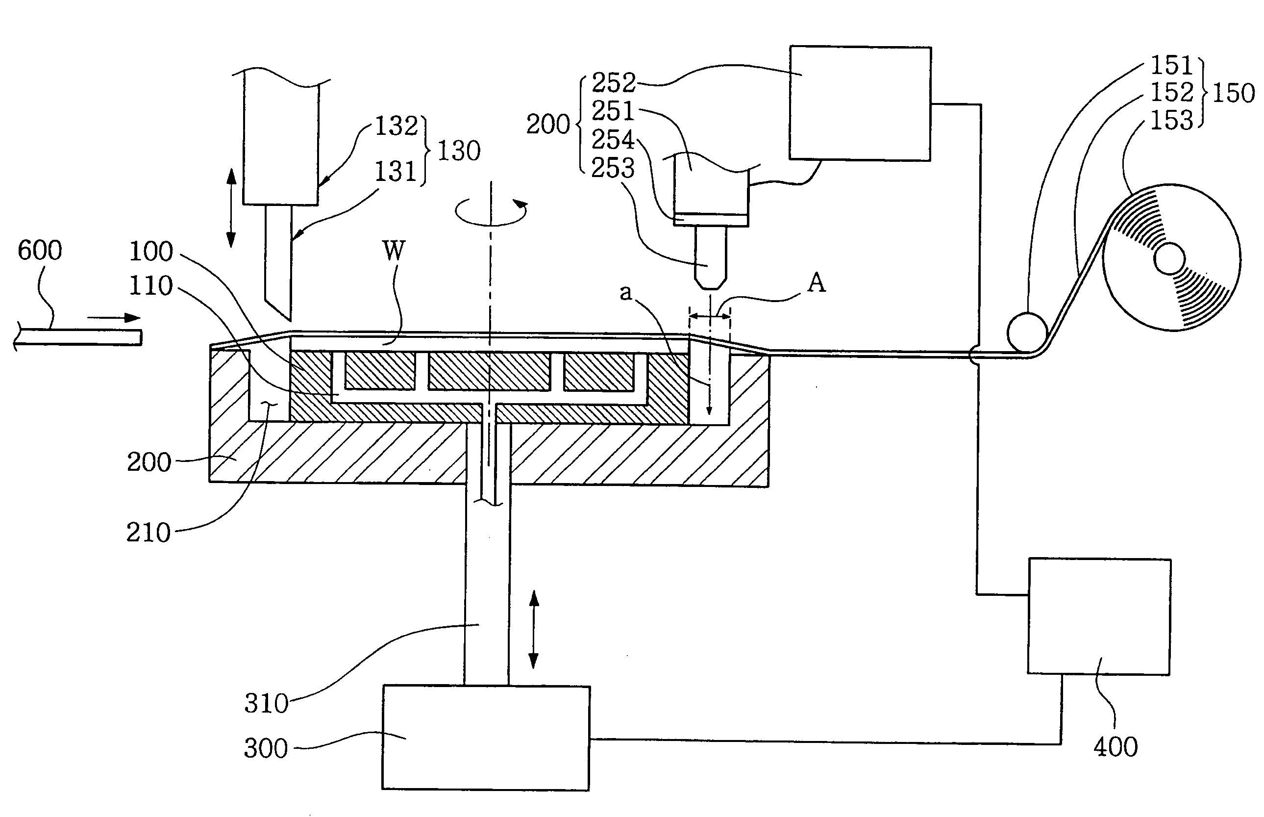
[0053]FIG. 3 is a sectional view illustrating a wafer protection tape cutting apparatus according to an embodiment of the present invention. FIG. 4 is a plan view illustrating protection tape on a top side of the wafer of FIG. 3.
[0054]Referring to FIGS. 3 and 4, the wafer protection tape cutting apparatus includes a chuck 100. A wafer W is held on the chuck 100. A vacuum hole 110 is formed in the chuck 100 and provides a bottom surface of the wafer W with a vacuum adsorption force. The vacuum hole 110 is connected to a vacuum supply unit (not shown) and receives the vac...
PUM
| Property | Measurement | Unit |
|---|---|---|
| Speed | aaaaa | aaaaa |
| Shape | aaaaa | aaaaa |
| Width | aaaaa | aaaaa |
Abstract
Description
Claims
Application Information