Liquid crystal device, projector, and electronic apparatus

a liquid crystal device and electronic equipment technology, applied in static indicating devices, instruments, non-linear optics, etc., can solve the problems of affecting the display or slow response speed, affecting the display effect, etc., to achieve fast response speed, excellent display characteristics, and effective fast bend transition

Inactive Publication Date: 2008-05-29
SEIKO EPSON CORP
View PDF5 Cites 5 Cited by
  • Summary
  • Abstract
  • Description
  • Claims
  • Application Information

AI Technical Summary

Benefits of technology

[0027]In this aspect, since the electronic apparatus includes the liquid crystal device which is capable of effectively performing fast bend tr

Problems solved by technology

If the initial transition manipulation is insufficient, transition from the splay alignment to the bend alignment is incompletely carried out, thereby resulting in defective display or slow response speed.
However, the technique disclosed in JP-A-2003-84299 has a problem in that light is blocked in a pixel in the case in which the control electrode overlaps the pixel electrode in a plan view because the control electrode is

Method used


Image

  • Liquid crystal device, projector, and electronic apparatus
  • Liquid crystal device, projector, and electronic apparatus
  • Liquid crystal device, projector, and electronic apparatus

Examples


second embodiment

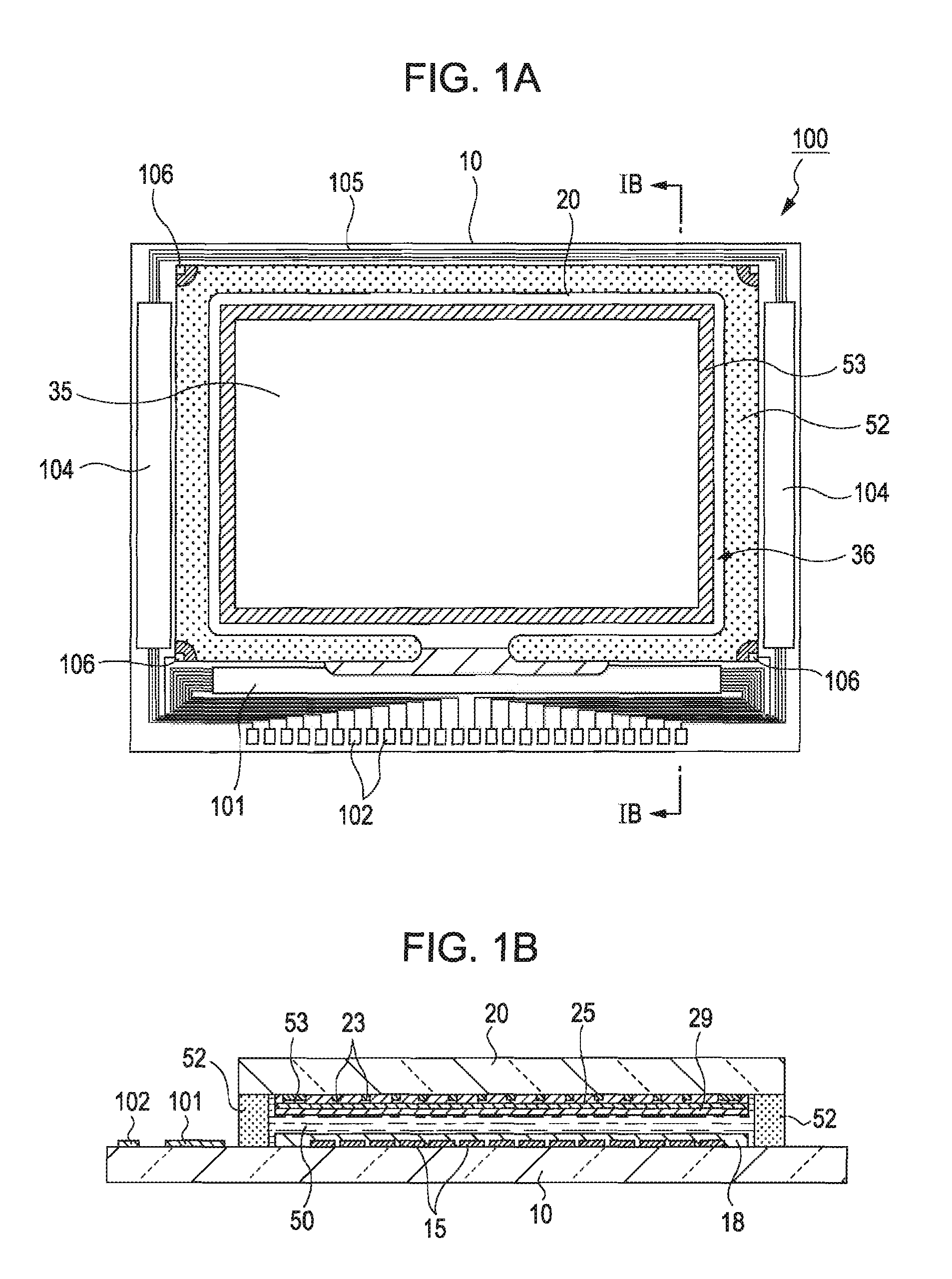
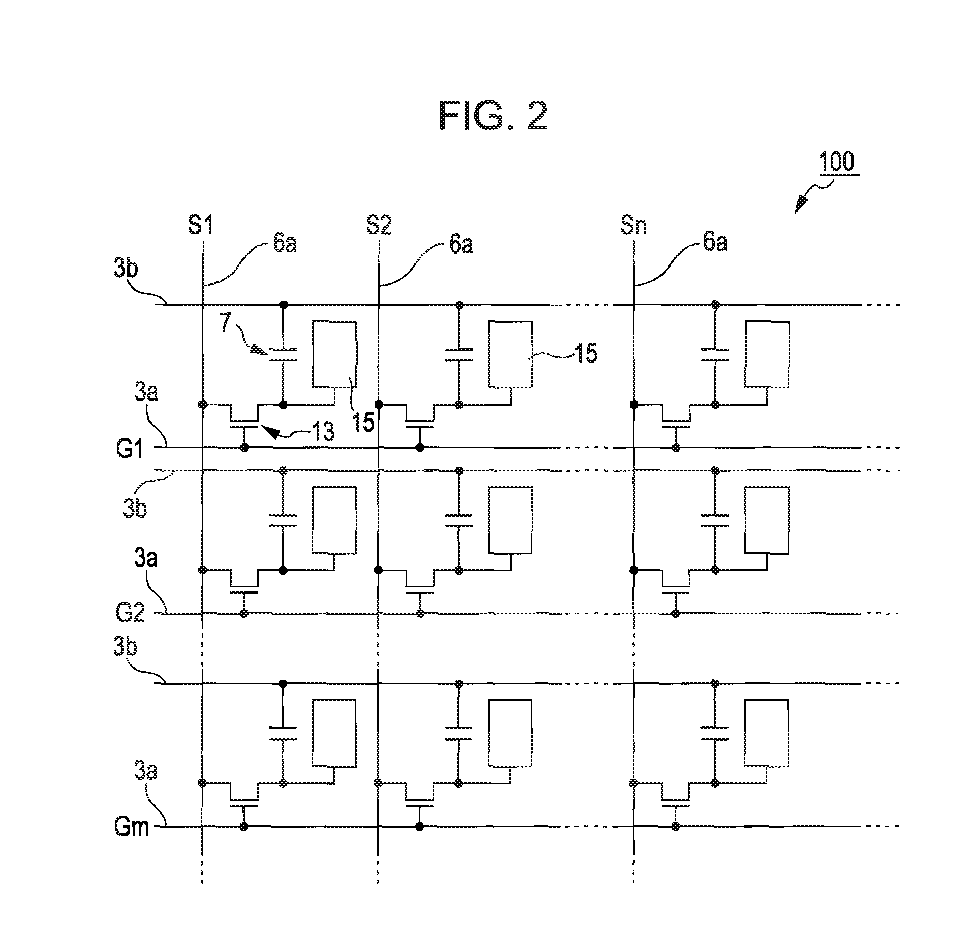
[0059]Hereinafter, a second embodiment of the invention will be described. In drawings relating to the second embodiment, a scale is arbitrarily determined for showing each element of a liquid crystal device in an enlarged manner so that the elements of the liquid crystal device are readily shown, like the first embodiment. Further, explanation of like elements in the first embodiment and the second embodiment will be omitted. The first embodiment and the second embodiment are different in the structure of the auxiliary electrode. Accordingly, the second embodiment will be described mainly with respect to the structure of the auxiliary electrode.

[0060]FIG. 6 shows a structure of a TFT array substrate 210 of a liquid crystal device 200 according to the second embodiment, and corresponds to FIG. 3A relating to the first embodiment. The TFT array substrate 210 is provided with a base layer and TFTs as in the first embodiment even though both are not shown. As shown in FIG. 6, an insula...

third embodiment

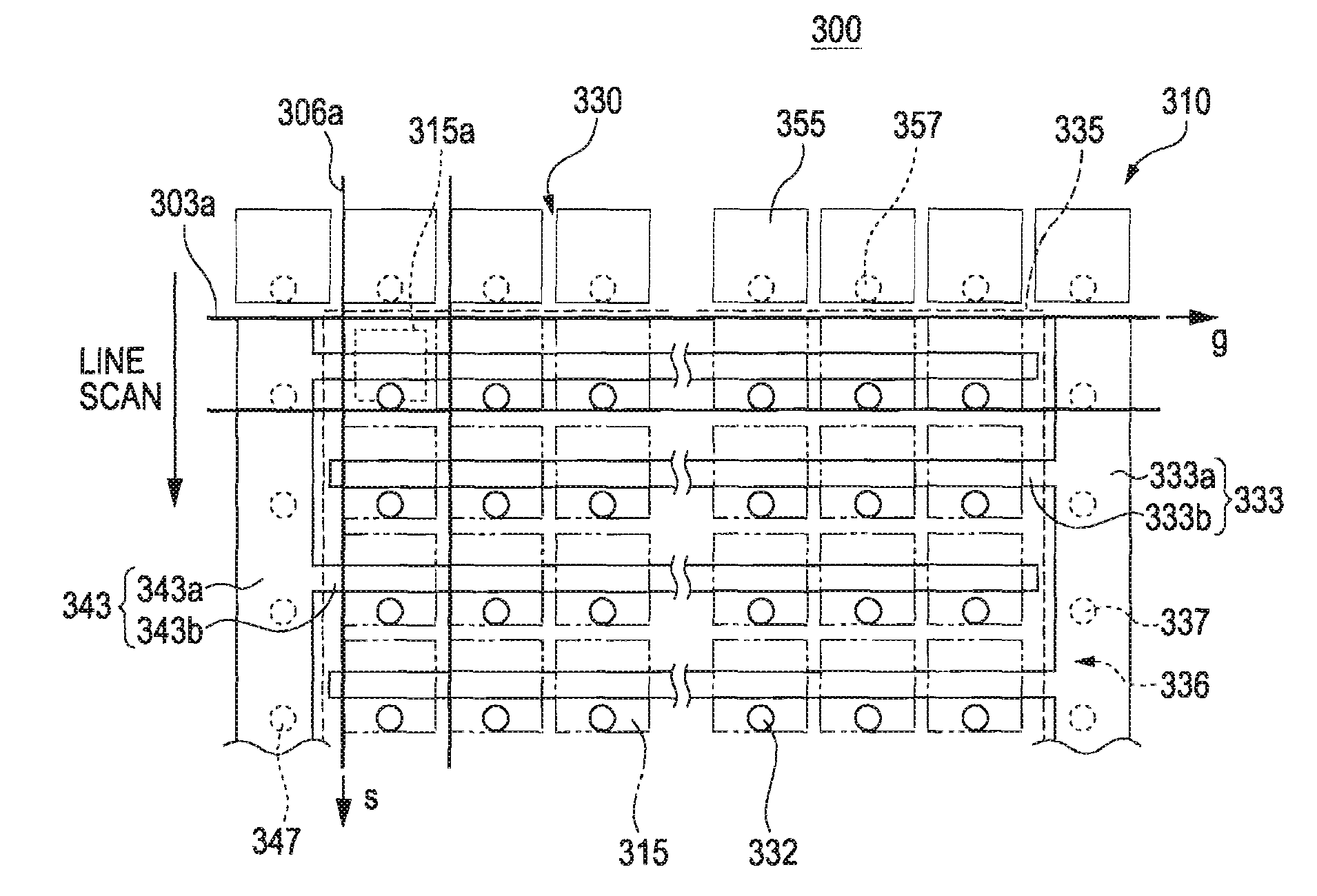
[0064]Hereinafter, a third embodiment of the invention will be described. In drawings relating to the third embodiment, a scale is arbitrarily determined for showing each element of a liquid crystal device in an enlarged manner so that the elements of the liquid crystal device are readily shown, like the first embodiment. Further, explanation about like elements in the first embodiment and the third embodiment will be omitted. The first embodiment and the third embodiment are different in the structure of the auxiliary electrode. Accordingly, the third embodiment will be described mainly with respect to the structure of the auxiliary electrode.

[0065]FIG. 7 shows a structure of a TFT array substrate 310 of a liquid crystal device 300 according to the third embodiment, and corresponds to FIG. 3A relating to the first embodiment. The TFT array substrate 310 is provided with a base layer and TFTs like the first embodiment even though both are not shown. As shown in FIG. 7, data lines 30...

fourth embodiment

[0072]Hereinafter, a fourth embodiment will be described. In drawings relating to the fourth embodiment, a scale is arbitrarily determined for showing each element of a liquid crystal device in an enlarged manner so that the elements of the liquid crystal device are readily shown, like the first embodiment. Further, explanation about like elements in the first embodiment and the fourth embodiment will be omitted. The first embodiment and the fourth embodiment are different in the structure of the auxiliary electrode. Accordingly, the fourth embodiment will be described mainly with respect to the structure of the auxiliary electrode.

[0073]FIG. 8 shows a structure of a TFT array substrate 410 of a liquid crystal device 400 according to the fourth embodiment. FIG. 8 is a plan view illustrating the TFT array substrate 410 of the liquid crystal device 400 and corresponds to FIG. 3A relating to the first embodiment. The TFT array substrate 410 is provided with a base layer, TFTs, and an i...


PUM


Abstract

A liquid crystal device has a pair of substrates arranged so as to face each other and a liquid crystal layer interposed between the pair of substrates and performs a display operation or an optical modulation operation by converting an alignment of liquid crystal molecules in the liquid crystal layer from a splay alignment to a bend alignment. The liquid crystal device includes a plurality of pixel electrodes disposed on either one of the pair of substrates so as to correspond to a plurality of pixels, and an auxiliary electrode formed in a layer disposed under the pixel electrodes in a manner such that at least part thereof overlaps the pixels in a plan view and made of a light-transmissible conductive material.

Description

BACKGROUND[0001]1. Technical Field[0002]The present invention relates to a liquid crystal device, a projector, and an electronic apparatus.[0003]2. Related Art[0004]In the field of a liquid crystal device for use in liquid crystal displays and projectors, there is a demand for picture quality improvement for moving images as well as still pictures. To obtain moving images with high quality, it is essential to improve the response time of a liquid crystal device. In recent years, optical compensated bend (OCB) mode liquid crystal devices have been attracting attention.[0005]In an OCB mode liquid crystal device, an alignment of liquid crystal molecules changes according to operation states, an initial state and a display state. In the initial state, liquid crystal molecules are controlled between two substrates such that the liquid crystal molecules are aligned in a splay form (splay alignment). However, in the display state, the liquid crystal molecules are controlled between two sub...

Claims


Application Information

Patent Timeline
IPC IPC(8): G02F1/13G02F1/1343
CPCG02F1/1395G02F2001/134318G09G2300/0491G09G3/3648G02F2001/134381G02F1/134318G02F1/134381
Inventor TSUCHIYA, YUTAKAUCHIDA, KOSUKE
Owner SEIKO EPSON CORP
Why Eureka
Try Eureka