Method of forming T- or gamma-shaped electrode

Inactive Publication Date: 2008-05-29
ELECTRONICS & TELECOMM RES INST
View PDF3 Cites 16 Cited by
  • Summary
  • Abstract
  • Description
  • Claims
  • Application Information

AI Technical Summary

Benefits of technology

[0014]The present invention is directed to a method of forming a gate electrode, which improves step coverage by a lithography process using a multi-layered photoresist layer wit

Problems solved by technology

Accordingly, in consideration of the size of an opening pattern and the thickness of the photoresist layer, it is difficult to control the height of the gate foot with respect to the fine gate pattern, and thus there m

Method used


Image

  • Method of forming T- or gamma-shaped electrode
  • Method of forming T- or gamma-shaped electrode
  • Method of forming T- or gamma-shaped electrode

Examples


Example

[0037]The present invention will now be described in more detail hereinafter with reference to the accompanying drawings, in which exemplary embodiments of the present invention are shown. The present invention may be embodied in various forms and not be limited to the exemplary embodiments described herein.

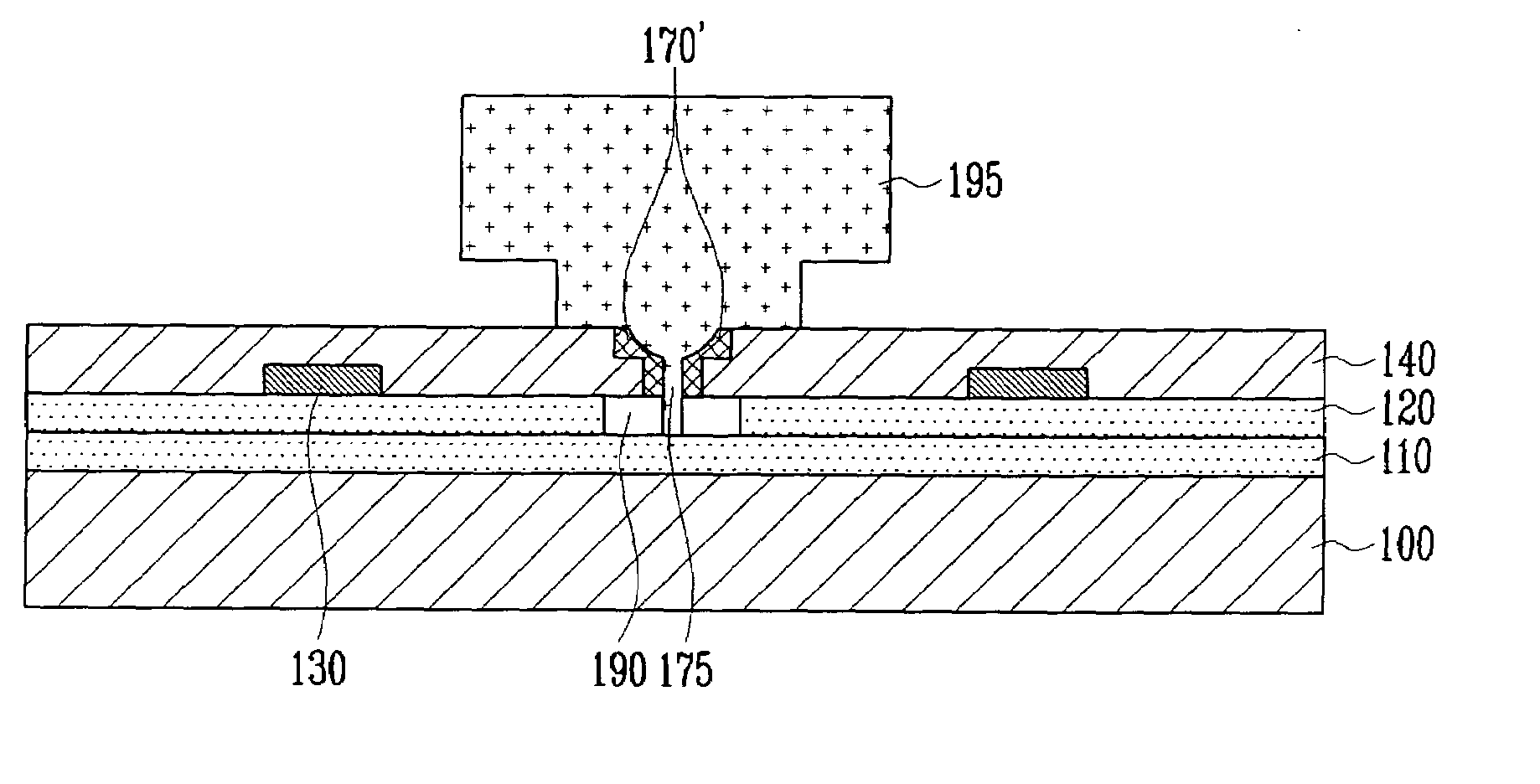
[0038]A method of forming a fine T-shaped gate electrode according to an exemplary embodiment of the present invention will now be described with reference to FIGS. 2A to 2K.

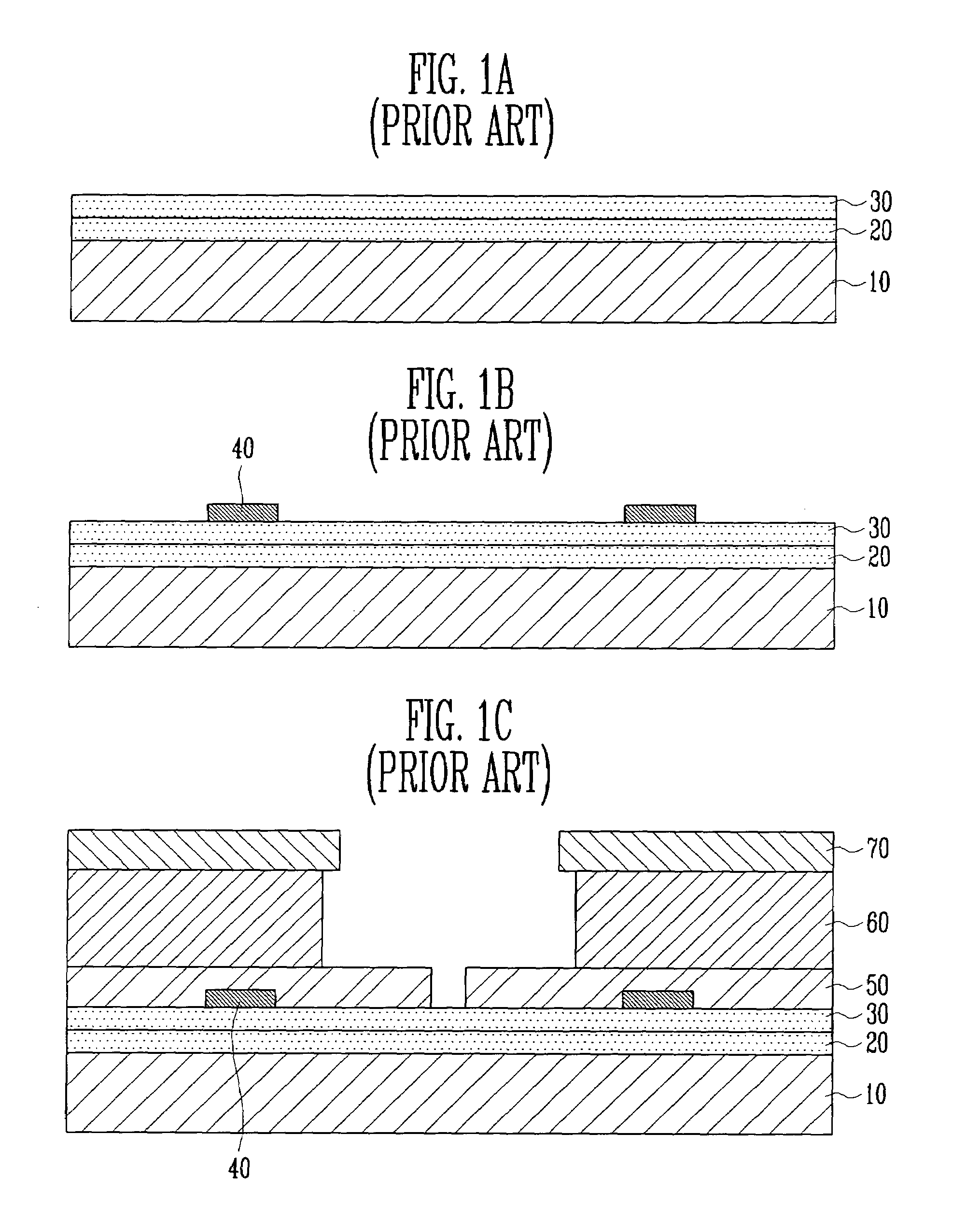
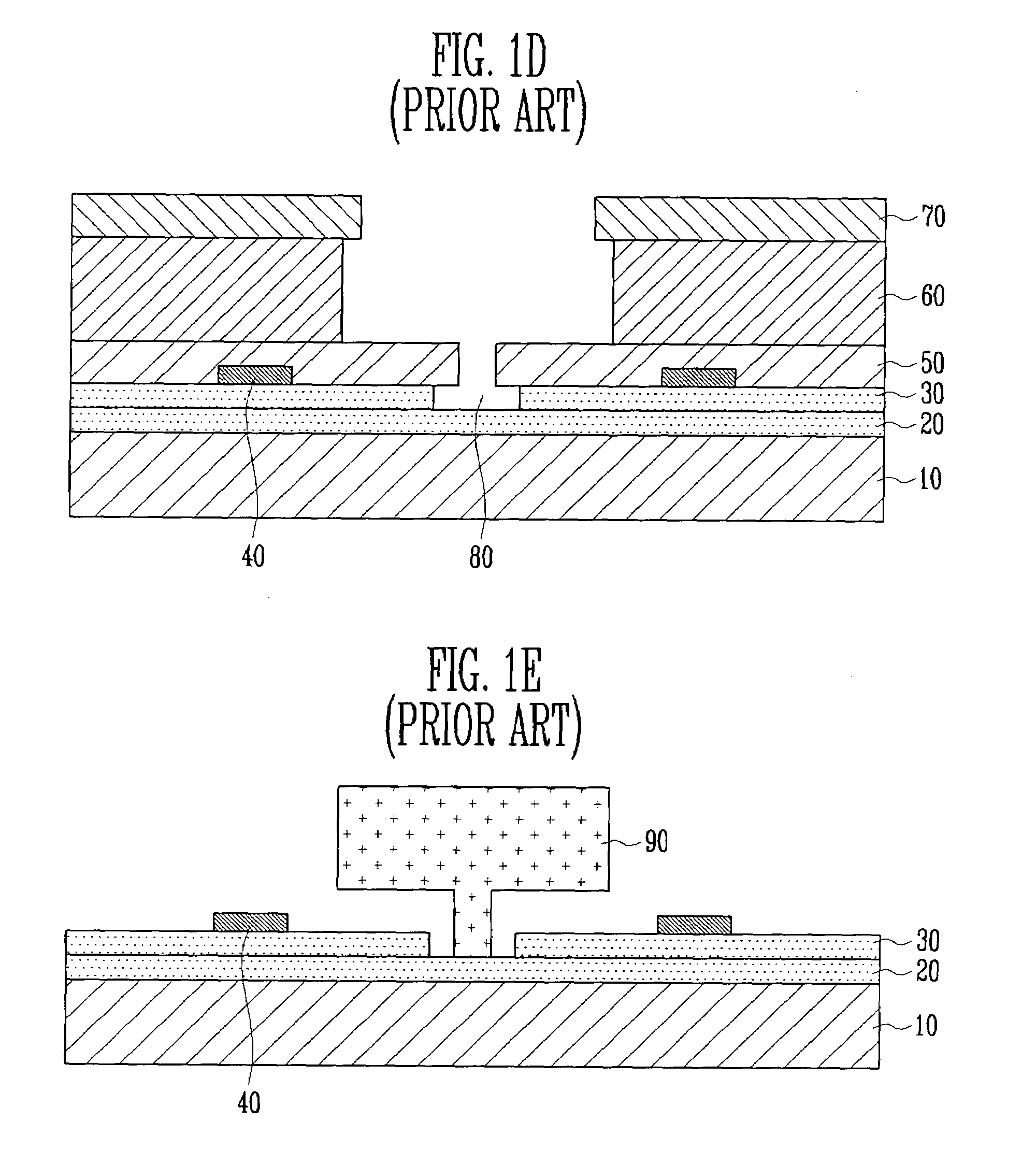
[0039]An active layer 110 and a capping layer 120 are first formed on a semiconductor substrate (in FIG. 2A), and a photoresist pattern then defines a region where an ohmic metal layer 130 which will serve as a source and a drain is to be formed. An ohmic metal is deposited, thereby forming an ohmic metal layer 130 through a process called rapid thermal annealing (RTA) (in FIG. 2B).

[0040]Here, the ohmic metal layer 130 may be a metal layer having a multi-layered structure in which AuGe, Ni and Au are deposite...


PUM


Abstract

A method of forming a fine T- or gamma-shaped gate electrode is provided, which is performed by a lithography process using a multi-layered photoresist layer having various sensitivities, deposition of an insulating layer, and an etching process. The method includes: a first step of depositing a first insulating layer on a semiconductor substrate; a second step of coating at least two photoresist layers with different sensitivities from each other on the first insulating layer, and patterning the photoresist layers to have openings which are different in size; a third step of etching the first insulating layer using the photoresist layers as etch masks to form a step hole in which a part contacting the substrate is narrower than an upper part thereof, and removing the photoresist layers; a fourth step of forming a photoresist layer on the first insulating layer, and forming an opening in the photoresist layer to have a T- or gamma-shaped gate head pattern; a fifth step of performing a gate recess process with respect to the gate pattern; and a sixth step of depositing a gate metal on the gate pattern, and removing the photoresist layers.

Description

CROSS-REFERENCE TO RELATED APPLICATION[0001]This application claims priority to and the benefit of Korean Patent Application No. 2005-114565, filed Nov. 29, 2006, the disclosure of which is incorporated herein by reference in its entirety.BACKGROUND[0002]1. Field of the Present Invention[0003]The present invention relates to a method of forming a gate electrode, and more particularly, to a method of forming a T- or gamma-shaped gate electrode.[0004]2. Discussion of Related Art[0005]Fine T- or gamma-shaped electrodes are gate electrodes widely employed in manufacturing a transistor that is used in the field using a high-frequency. As semiconductor devices are highly integrated, there are various researches on a method of forming an electrode which can reduce the length of a gate, has excellent high frequency characteristics, and does not deteriorate gain or noise characteristics.[0006]A conventional process of forming such a T- or gamma-shaped electrode will now be descried with refe...

Claims


Application Information

Patent Timeline
IPC IPC(8): H01L21/338
CPCH01L21/28587H01L29/4232H01L21/28593H01L29/42376H01L29/66621H01L21/28114H01L21/31144
Inventor AHN, HO KYUNLIM, JONG WONMUN, JAE KYOUNGCHANG, WOO JINJI, HONG GUKIM, HAE CHEON
Owner ELECTRONICS & TELECOMM RES INST
Why Eureka
Try Eureka