Metallization method of semiconductor device
- Summary
- Abstract
- Description
- Claims
- Application Information
AI Technical Summary
Benefits of technology
Problems solved by technology
Method used
Image

Examples
Embodiment Construction
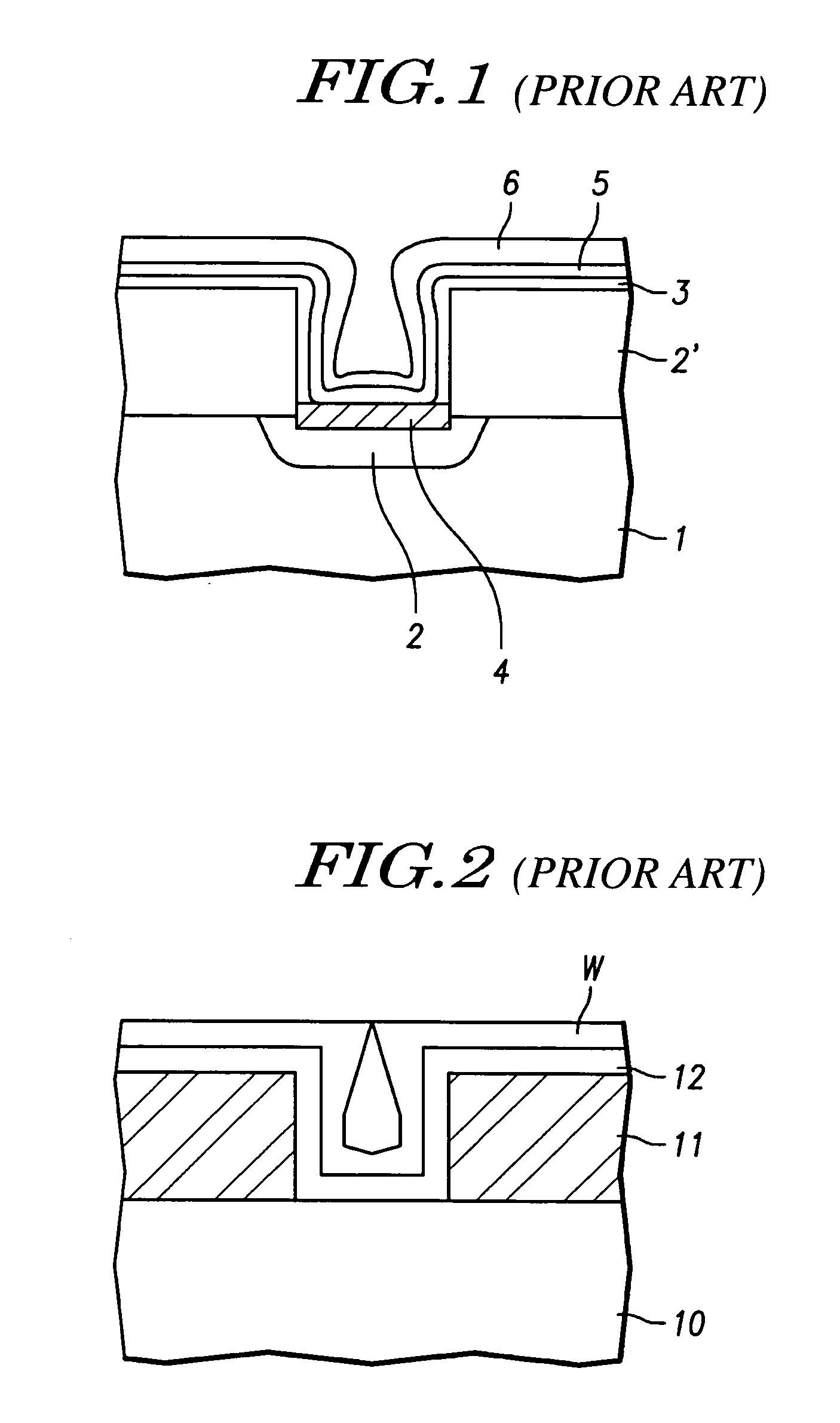
[0020] Reference will now be made in detail to the present embodiments of the invention, examples of which are illustrated in the accompanying drawings. Wherever possible, the same reference numbers will be used throughout the drawings to refer to the same or like parts.
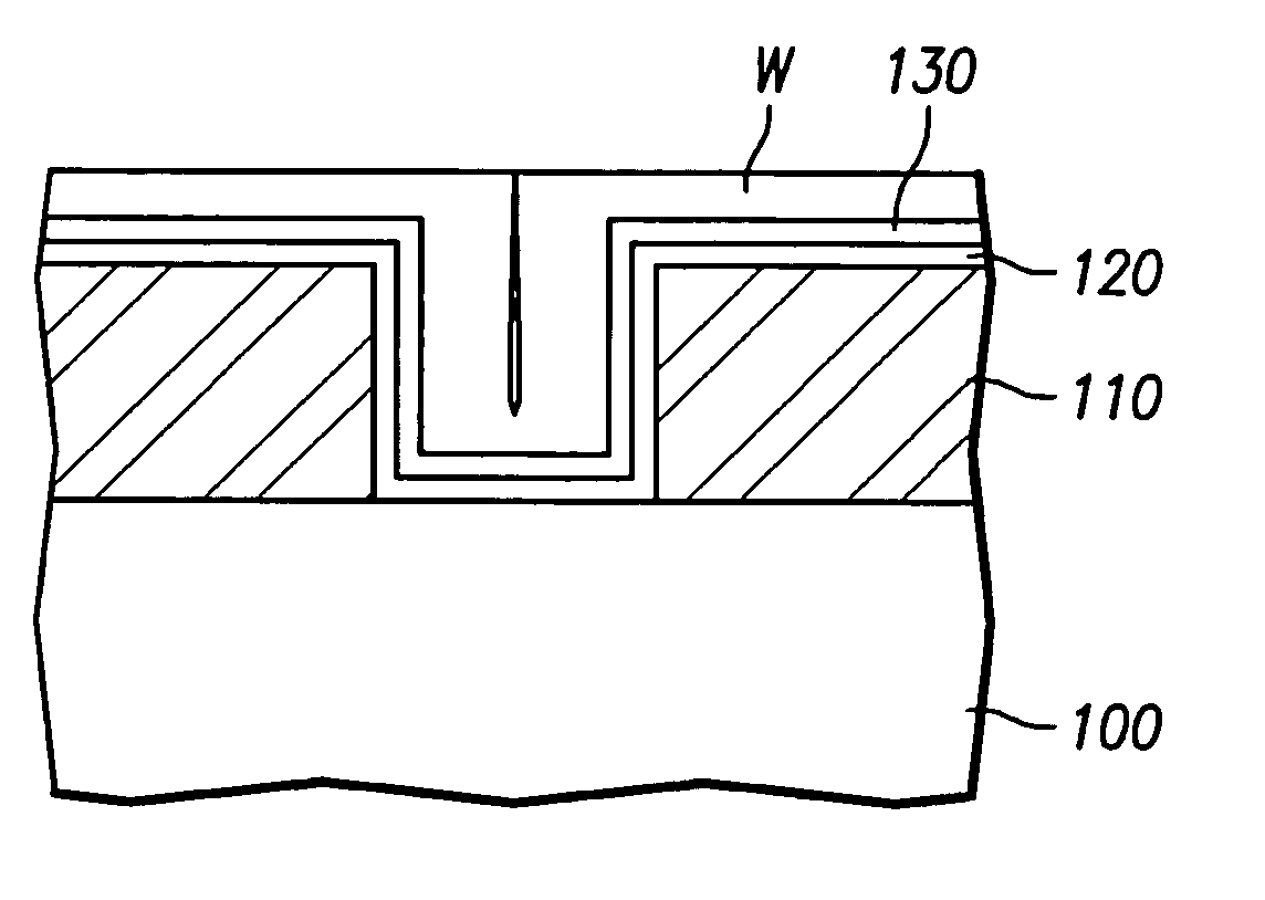
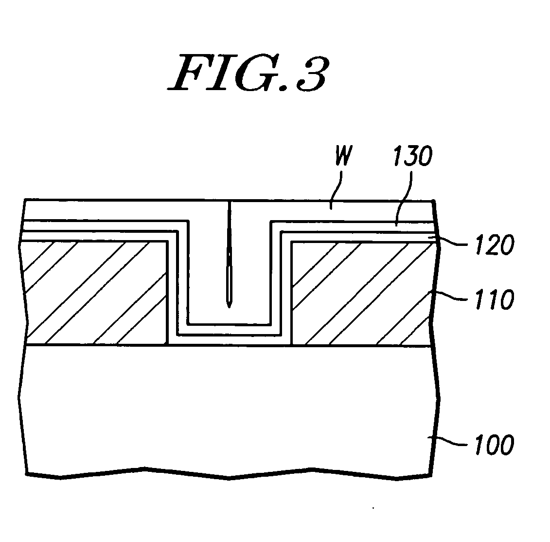
[0021]FIG. 3 illustrates an exemplary contact structure utilizing a bilayer TiN barrier structure with a tungsten contact layer. The bilayer TiN structure comprises one TiN layer deposited by a chemical vapor deposition (CVD) process and one TiN layer deposited by a physical vapor deposition (PVD) process. The CVD TiN layer may be formed to have a minimum thickness and may have an amorphous or non-crystalline structure.
[0022] Referring to FIG. 3, a contact hole (or via hole, not numbered) is formed by etching a predetermined portion of an insulating layer 110 formed on a silicon substrate 100. The contact hole exposes a portion of an active region of substrate 100. A TiN layer 120 is then formed by CVD, to a thickn...
PUM
 Abstract
Description
Claims
Application Information
 - Generate Ideas
- Intellectual Property
- Life Sciences
- Materials
- Tech Scout
- Unparalleled Data Quality
- Higher Quality Content
- 60% Fewer Hallucinations
Browse by: Latest US Patents, China's latest patents, Technical Efficacy Thesaurus, Application Domain, Technology Topic, Popular Technical Reports.
© 2025 PatSnap. All rights reserved.Legal|Privacy policy|Modern Slavery Act Transparency Statement|Sitemap|About US| Contact US: help@patsnap.com