
Crystalline Semicondutor Film and Method for Manufacturing the Same

Active Publication Date: 2009-06-04
SHARP KK
View PDF7 Cites 12 Cited by
  • Summary
  • Abstract
  • Description
  • Claims
  • Application Information

AI Technical Summary

Benefits of technology

[0041]According to the present invention, the islands of a crystalline semiconductor have a gently sloped shoulder portion (i.e., the junction between the body portion and the edge portion). Thus, by using a TFT including such a crystalline semiconductor film, a high-performance semiconductor device, in which the generation of leakage current is minimized and of which the gate insulating film has increased breakdown voltage and improved step coverage, is realized.
[0042]In addition, according to the present invention, both the crystal grains in the body portion and the crystal grains in the edge portion have average grain sizes that are greater than 0.2 μm, and preferably have substantially the same average grain size. That is to say, the overall crystalline semiconductor film preferably has a uniform grain size. That is why by using a TFT including such a crystalline semiconductor film, not only the effects described above but also uniform field effect mobility and constant TFT off-state current are achieved as well. As a result, a high-performance semiconductor device with low power dissipation is realized.
[0043]Furthermore, according to the present invention, an amorphous semiconductor film, to which a catalyst element that promotes crystallization has been added, is used, thereby obtaining a quality crystalline semiconductor film with aligned crystallographic orientations. And by fabricating a TFT with such a crystalline semiconductor film, a high-performance semiconductor device that exhibits stabilized characteristics can be obtained with variations in TFT characteristics reduced.
[0044]Consequently, by using the crystalline semiconductor film of the present invention, a high-performance semiconductor device is realized. Particularly when this semiconductor film is applied to an LCD, the switching characteristic of pixel switching TFTs can be improved as required in an active-matrix substrate and yet the performance of TFTs that form a peripheral driver circuit section can also be improved as well. As a result, in a driver monolithic active-matrix substrate including an active-matrix section and a peripheral driver circuit section on the same substrate, the size of the module can be reduced and the performance thereof can be improved.
[0045]The present invention is applicable for use in active-matrix-addressed LCDs, organic EL displays, close-contact image sensors and three-dimensional ICs, for example.

Problems solved by technology

And unless that huge amount of information is written in a short time, it is impossible to present the image, having an enormous amount of information to realize high-definition video, cannot be presented as moving pictures, for example.
However, it is known that according to such a method of crystallizing an amorphous semiconductor film or recrystallizing a crystalline semiconductor film by irradiating the film with a laser beam and melting and solidifying the film, the surface of the resultant crystalline semiconductor film will get uneven.
For example, since the top (or edge) of the ridge is sharp, the electric field is often concentrated there to generate leakage current, decrease the breakdown voltage of the gate insulating film, and eventually deteriorate the overall reliability of the device including hot carrier resistance.
On top of that, if there is a ridge, the gate insulating film, deposited by a sputtering process or a CVD process, has decreased step coverage to make the electrical insulation insufficient.
Furthermore, if the device is a top gate type thin-film transistor, the ridge will be located in the interface between the gate insulating film and the channel, and therefore, may sometimes affect the interface characteristic or decrease the field effect mobility.

Method used


Image

  • Crystalline Semicondutor Film and Method for Manufacturing the Same
  • Crystalline Semicondutor Film and Method for Manufacturing the Same
  • Crystalline Semicondutor Film and Method for Manufacturing the Same

Examples


Embodiment Construction

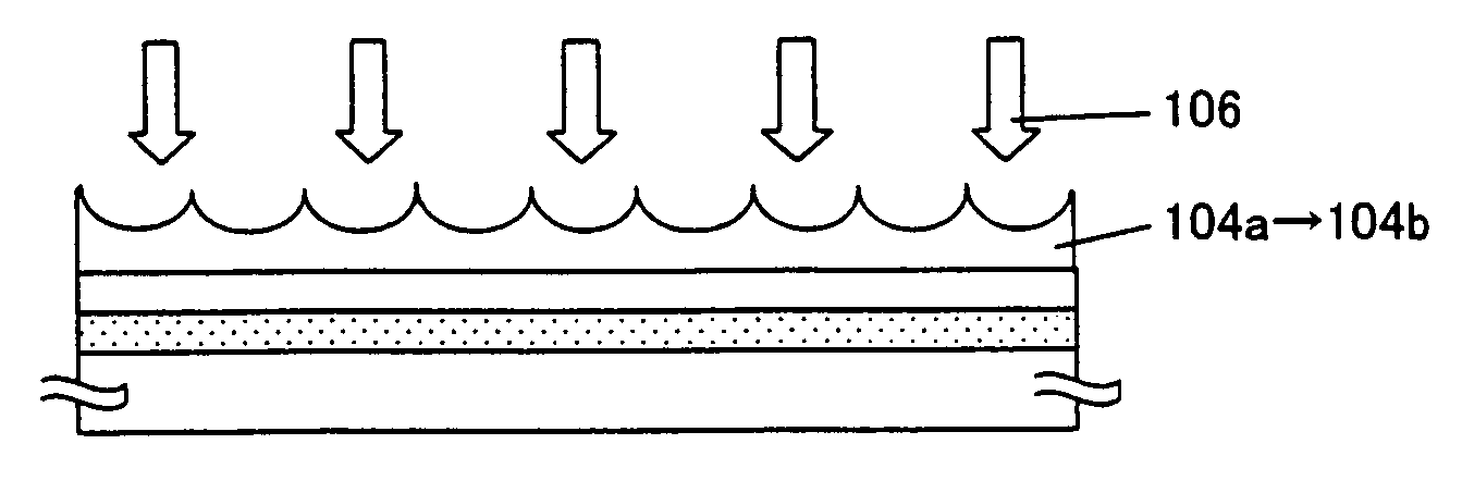
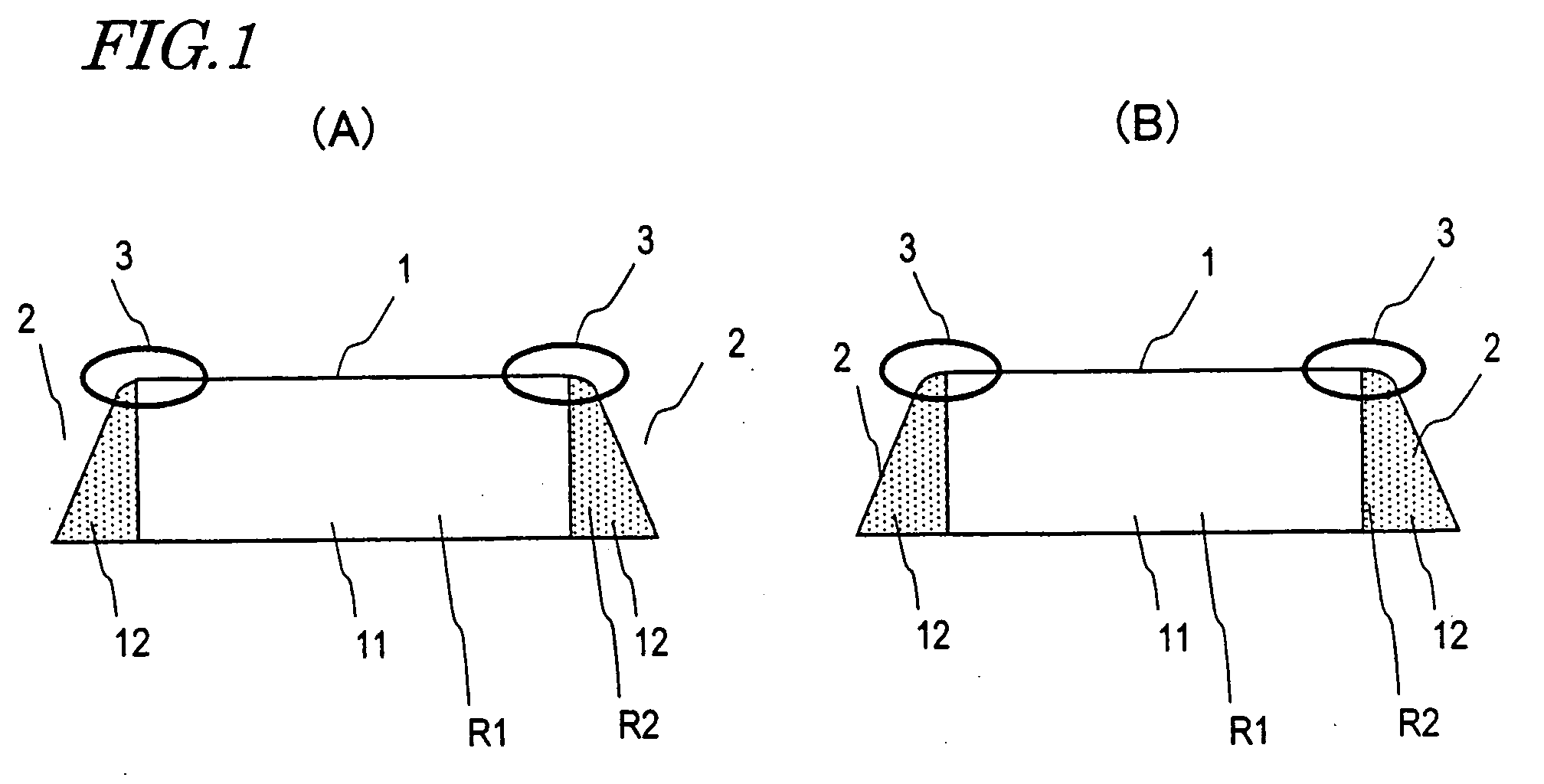
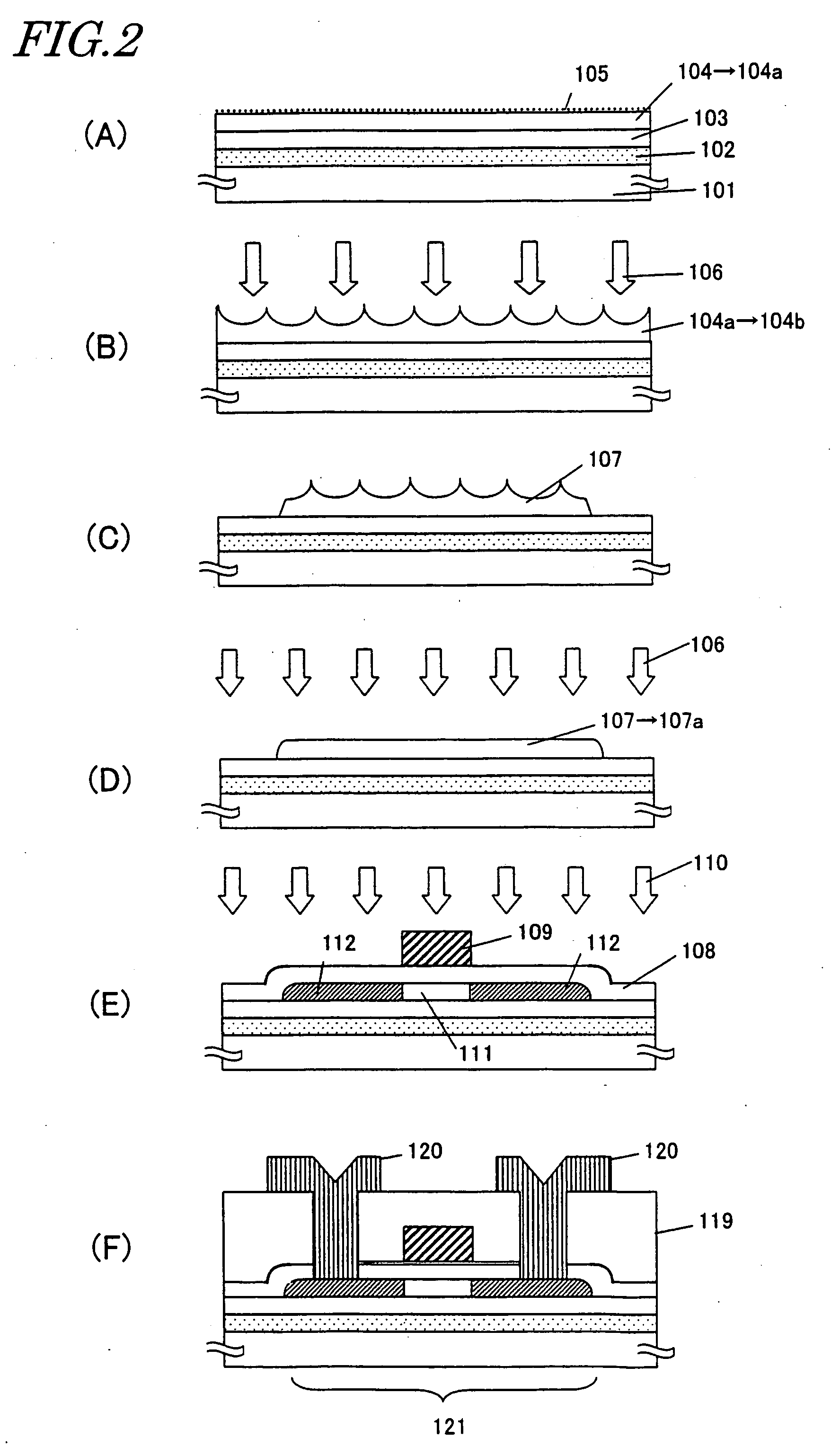
[0080]To realize a TFT (a kind of semiconductor device) of which the gate insulating film has a high breakdown voltage and good step coverage by minimizing the generation of leakage current, the present inventors tried to find the reason why the desired TFT characteristics could not be achieved by the methods disclosed in Patent Documents Nos. 2 to 4 mentioned above. This is because as the surface of a crystalline semiconductor film formed by any of these methods has been flattened by reducing the ridges, the breakdown voltage of the gate insulating film should be improvable, theoretically speaking. As a result, the present inventors discovered that to realize a TFT with desired characteristics, it was not enough to just flatten the surface of the crystalline semiconductor film but it was also important to form islands of a crystalline semiconductor, of which the body and edge portions were joined together with a gently curved surface and which had a uniform crystal grain size over ...


PUM


Abstract

An island of a crystalline semiconductor according to the present invention has an upper surface and a sloped side surface, which are joined together with a curved surface. Crystal grains in a body portion of the island, including the upper surface, and crystal grains in an edge portion of the island, including the sloped side surface, both have average grain sizes that are greater than 0.2 μm.

Description

TECHNICAL FIELD[0001]The present invention relates to a crystalline semiconductor film, a method of making such a film, and a semiconductor device to be fabricated with the crystalline semiconductor film.BACKGROUND ART[0002]Recently, to realize an LCD or an organic EL display of a huge size and with high resolution, a high-speed and high-resolution image sensor, a three-dimensional IC and so on, research and development of fabricating high-performance semiconductor devices on either an insulating substrate such as a glass substrate or an insulating film has been carried on. Among other things, an LCD, including pixel portions and a driver on the same substrate, has been used as a monitor for not only personal computers (PCs) but also other general consumer electronic appliances. For example, more and more cathode-ray tubes (CRTs) have been replaced with LCDs as TV monitors and front projectors for viewing movies or enjoying games for amusement purposes have been purchased by an incr...

Claims


Application Information

Patent Timeline
IPC IPC(8): H01L29/04H01L21/70
CPCH01L21/02532H01L21/02672H01L21/02686H01L27/1285H01L29/66757H01L29/78675H01L27/1277H01L29/04
Inventor KIMURA, TOMOHIROYASUMATSU, TAKUTO
Owner SHARP KK
Features
  • Generate Ideas
  • Intellectual Property
  • Life Sciences
  • Materials
  • Tech Scout
  • Unparalleled Data Quality
  • Higher Quality Content
  • 60% Fewer Hallucinations
Learn More