FET device manufacturing using a modified Ion implantation method

Inactive Publication Date: 2018-03-22
GUILLEN PEDRO
View PDF1 Cites 0 Cited by
  • Summary
  • Abstract
  • Description
  • Claims
  • Application Information

AI Technical Summary

Benefits of technology

[0012]An object of the invention is to provide a method for manufacturing a semiconductor device exhibit

Problems solved by technology

Such a conventional method for manufacturing a semiconductor device has problems.
As a result, it is hard to adjust threshold voltage using the p

Method used


Image

  • FET device manufacturing using a modified Ion implantation method
  • FET device manufacturing using a modified Ion implantation method
  • FET device manufacturing using a modified Ion implantation method

Examples


Embodiment Construction

[0019]Reference will now be made in detail to the preferred embodiments of the present invention, examples of which are illustrated in the accompanying drawings.

[0020]Referring to FIGS. 2a to 2e, there is provided a manufacturing method of a semiconductor device.

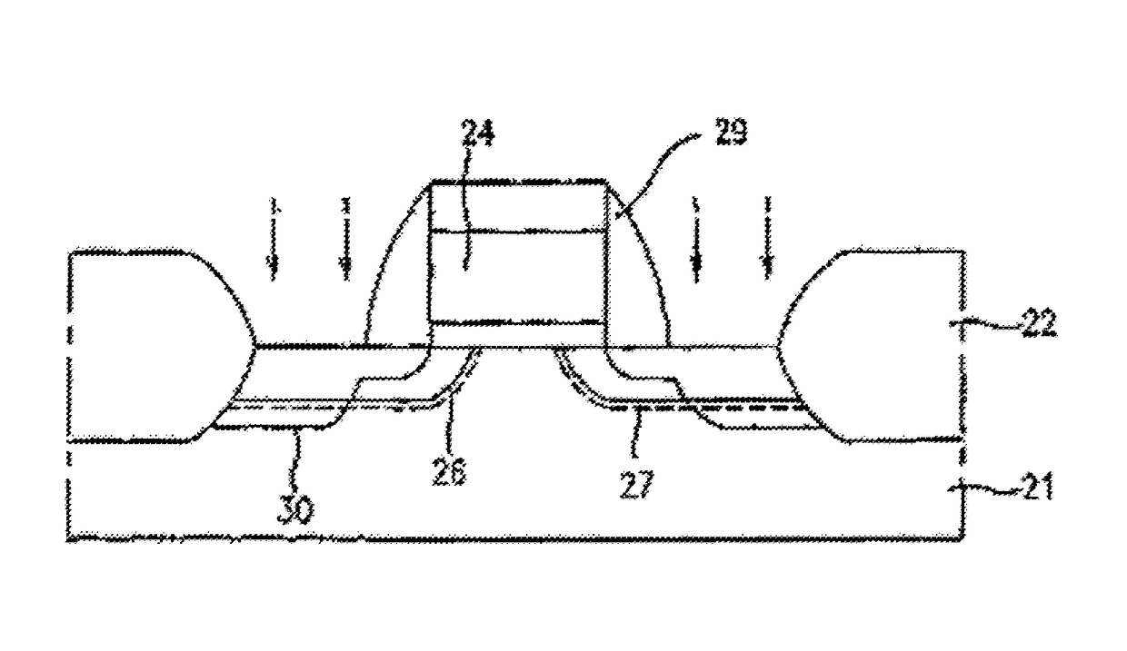
[0021]Referring to FIG. 2a, field regions and active regions are defined on a semiconductor substrate 21, e.g., P-type monocrystalline silicon. Then a field oxide layer 22 is formed on the field regions.

[0022]Subsequently, a first oxide layer, a conductive (e.g., polysilicon) layer, and an insulating layer are successively formed. The insulating layer is an oxide layer, a nitride layer, a doped oxide layer, or double layers of an oxide and a nitride. Utilizing a mask, the first oxide layer, the polysilicon layer, and the insulating layer are patterned to form a gate insulating (e.g., oxide) layer 23, a gate electrode 24, and a gate cap insulating layer 25.

[0023]Referring to FIG. 2b, using the gate electrode 24 as a mask, one...


PUM


Abstract

A method for manufacturing a semiconductor device exhibiting improved short channel effects and increased current driving ability is disclosed. The method includes the steps of: providing a substrate of a first conductivity-type, e.g., P-type; forming a gate insulating layer on the substrate; forming a gate electrode on the gate insulating layer; forming a gate cap insulating layer on the gate electrode; introducing inactive ions of the first conductivity-type into the first conductivity-type semiconductor substrate at both sides of the gate electrode, so as to form amorphous regions; forming first impurity regions of the first conductivity-type near the amorphous regions; and forming second impurity regions of a second conductivity-type, e.g., N-type, in the substrate at both sides of the gate electrode. The method also includes forming source and drain regions of the second conductivity-type in the substrate. The amorphous regions are formed by ion implantation of the inactive ions while the first and second impurity regions and the source and drain regions are formed by ion implantation of active ions. Inactive ions are ions which, after implantation into the amorphous regions, assume an atomic or molecular state in which they act neither as acceptors nor donors. Conversely, active ions act as acceptors or donors after implantation.

Description

FIELD OF THE INVENTION[0001]The present invention relates to a method for manufacturing a semiconductor device exhibiting improved short channel effects and increased current driving ability.BACKGROUND OF THE INVENTION[0002]A conventional method for manufacturing a semiconductor device will be discussed with reference to the attached drawings.[0003]FIGS. 1a to 1d are cross-sectional views showing a conventional method for manufacturing a semiconductor device.[0004]As shown in FIG. 1a, active regions and field regions are defined on a P-type semiconductor substrate 1. A field oxide layer 2 is formed on the field regions. Subsequently, a first oxide layer, a polysilicon layer and a second oxide layer are successively formed on the entire surface. Utilizing a mask, the first oxide layer, the polysilicon layer, and the second oxide layer are patterned to form a gate oxide layer 3, a gate electrode 4, and a gate cap insulating layer 5. P-type impurity ions are implanted at a tilt angle o...

Claims


Application Information

Patent Timeline
IPC IPC(8): H01L29/66H01L21/265H01L21/225H01L21/324H01L29/10H01L29/78
CPCH01L29/66537H01L29/66598H01L21/26513H01L29/7833H01L21/2253H01L21/324H01L29/1083H01L21/26533H01L21/26506H01L29/6659H01L29/1041H01L21/26586
Inventor GUILLEN, PEDRO
Owner GUILLEN PEDRO
Why Eureka
Try Eureka