

Semiconductor device
- Summary
- Abstract
- Description
- Claims
- Application Information
AI Technical Summary
Benefits of technology
Problems solved by technology
Method used
Image

Examples
first preferred embodiment
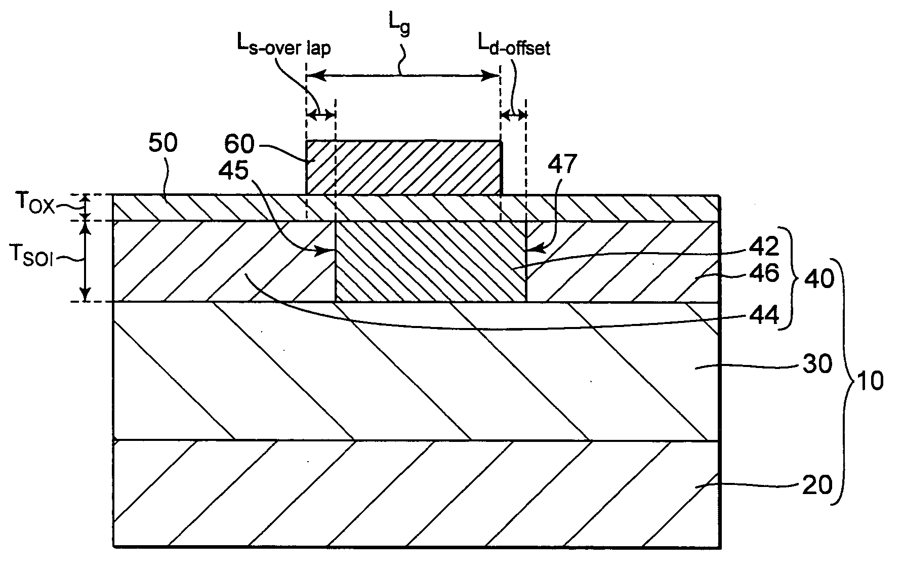
[0046] An MOSFET (Metal-Oxide-Semiconductor Field Effect Transistor) using an SOI (Silicon On Insulator) substrate will be explained as a semiconductor device according to a first embodiment with reference to FIG. 1. FIG. 1 is a schematic diagram for describing one example of a structure of the semiconductor device according to the first embodiment and shows it in the form of a cut area of its section.
[0047] The SOI substrate 10 may use an arbitrary suitable one known to date. In the SOI substrate 10, a buried oxide film (BOX) layer 30 used as an insulating layer and an SOI layer 40 are sequentially laminated over a silicon substrate 20 used as a semiconductor substrate.
[0048] A source region 44 and a drain region 46 are respectively provided in the SOI layer 40 as n-type impurity diffusion regions in discrete form. An impurity introduction-free non-doped region 42 is provided at a position interposed between the source and drain regions 44 and 46 in the SOI layer 40. The non-dope...
second preferred embodiment
[0063] An MOSFET using an SOI substrate will be explained as a semiconductor device according to a second embodiment with reference to FIG. 5. FIG. 5 is a schematic diagram for explaining one example of a structure of the semiconductor device according to the second embodiment and shows it in the form of a cut area of its section.
[0064] The SOI substrate 10 may use an arbitrary suitable one known to date. In the SOI substrate 10, a buried oxide film (BOX) layer 30 used as an insulating layer and an SOI layer 40 are sequentially laminated over a silicon substrate 20 used as a semiconductor substrate.
[0065] A source region 44 and a drain region 46 are respectively provided in the SOI layer 40 as n-type impurity diffusion regions in discrete form. An impurity introduction-free non-doped region 42 is provided at a position interposed between the source and drain regions 44 and 46 in the SOI layer 40.
[0066] A gate electrode 61 is formed on the upper side of the SOI layer 40 with a gat...
PUM
 Abstract
Description
Claims
Application Information