Method for forming semiconductor wafer having insulator

a technology of insulator and semiconductor wafer, which is applied in the direction of semiconductor devices, basic electric elements, electrical equipment, etc., can solve the problems of increasing the mobility of moving electrons, increasing the cost of manufacturing, and increasing the deterioration of the oxide layer

Inactive Publication Date: 2007-07-05
DONGBU ELECTRONICS CO LTD
View PDF4 Cites 0 Cited by
  • Summary
  • Abstract
  • Description
  • Claims
  • Application Information

AI Technical Summary

Benefits of technology

[0010] Accordingly, the present invention has been made to solve the above-mentioned problems occurring in the prior art, and an object of the present invention is to provide a MOS transistor, which can solve punch through due to a short channel effect, DIBL and leakage current by forming an insulating layer pattern in the lower portion of a device by using polymer and silicon germanium.

Problems solved by technology

Further, Hot Carrier Injection (HCI) has occurred, in which mobility of moving electrons excessively increases due to high electric field.
Furthermore, lifetime reduction has occurred due to deterioration of a gate oxide layer.
The oxide layer is increasingly deteriorated due to holes injected into the gate oxide layer from a p-type wafer.
However, it has a severe floating body effect in which holes generated by collision transition are stacked in the neutral region and thus increase the potential of the body.

Method used


Image

  • Method for forming semiconductor wafer having insulator
  • Method for forming semiconductor wafer having insulator
  • Method for forming semiconductor wafer having insulator

Examples


Embodiment Construction

[0017] Hereinafter, an embodiment of the present invention will be described with reference to the accompanying drawings.

[0018] In the following description, technical contents will be omitted that are well known in the field of the present invention and have no direct relation to the present invention. This is for more clearly transferring the subject matter of the present invention by omitting an unnecessary description. For the same reason, some elements are enlarged, omitted or schematically illustrated in the accompanying drawings. The size of each element is not shown in the real size.

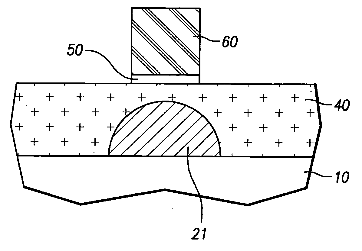
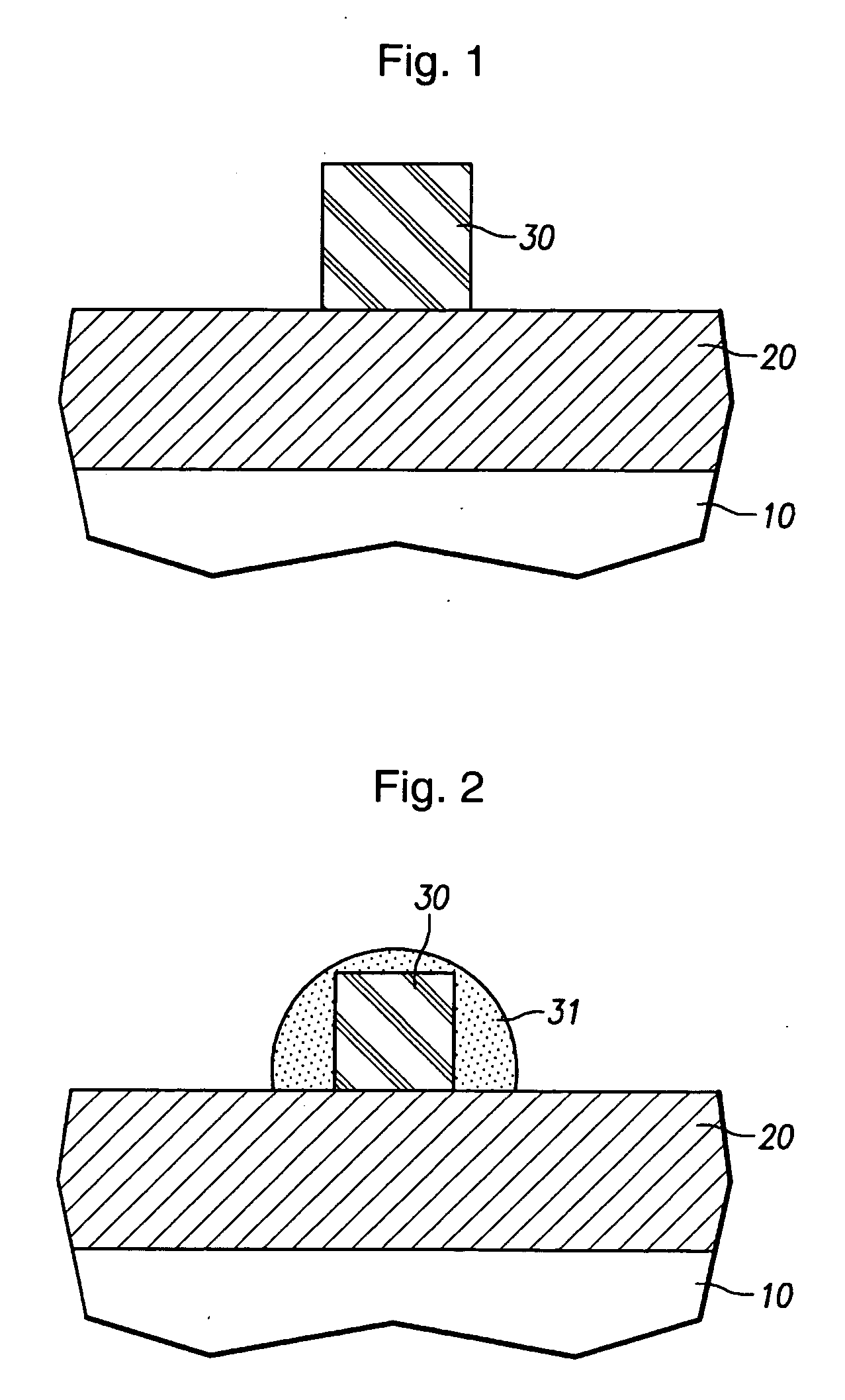
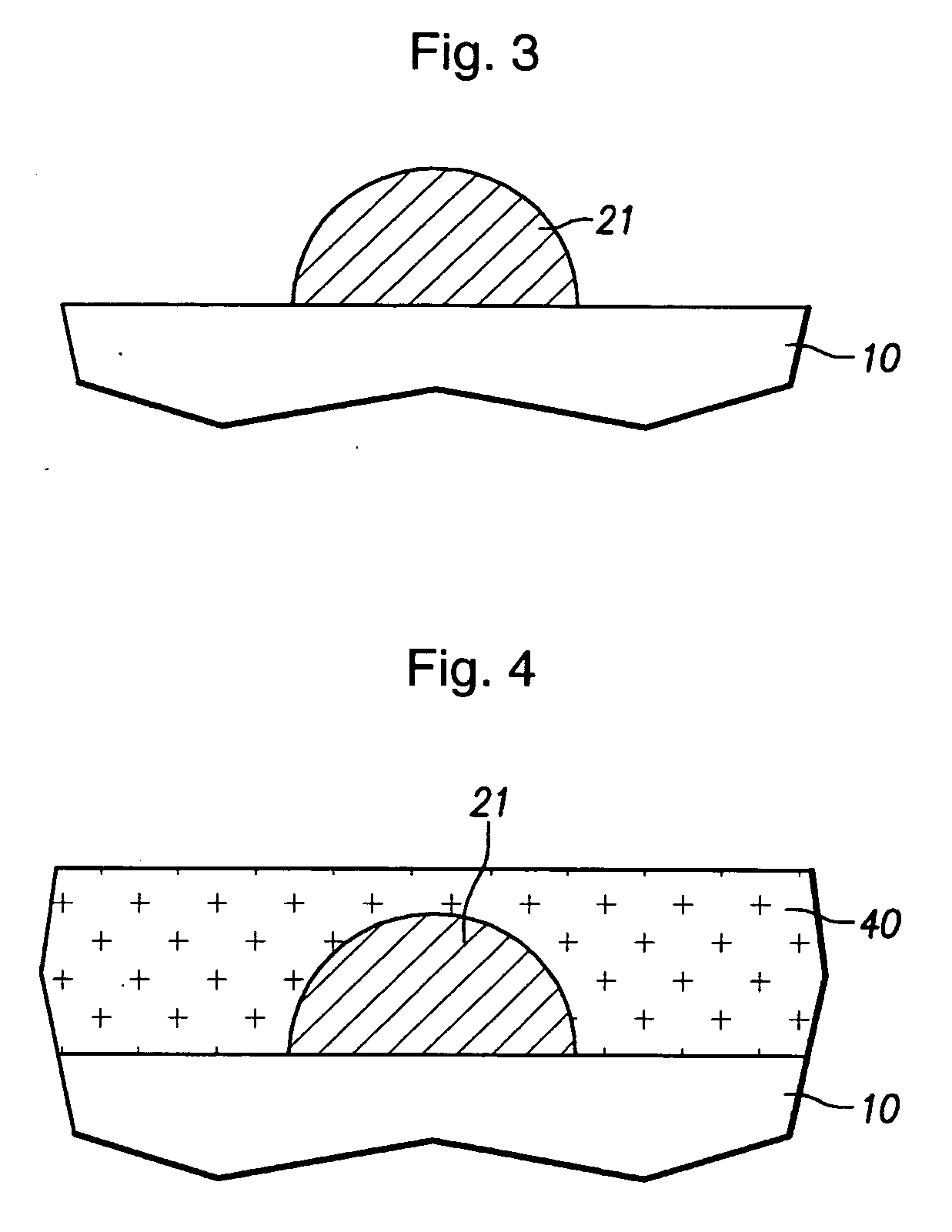
[0019] FIGS. 1 to 5 are sectional views according to steps illustrating a method for forming a semiconductor wafer having an insulator according to one embodiment of the present invention.

[0020] Referring to FIG. 1, an insulating layer 20 is formed on a silicon wafer 10. For example, the insulating layer 20 is formed using a thermal oxidation method, a Low Pressure Chemical Vapor Deposition (L...


PUM


Abstract

Provided is a method for forming a semiconductor wafer having an insulator. According to the method, an insulating layer pattern and a silicon germanium layer are formed on a wafer, and a structure similar to a SOI wafer is formed. Accordingly, since the thin insulating layer pattern exists between the surface of the wafer, in which a circuit is formed, and a lower layer thereof, parasitic capacitance is reduced and thus device performance can be improved. In addition, punch through due to a short channel effect, DIBL and leakage current can be solved as with the SOI wafer. Further, the insulating layer pattern is formed instead of an insulating layer formed on the SOI wafer, so that holes are prevented from being stacked in a neutral region. Consequently, a floating body effect can be prevented from occurring.

Description

BACKGROUND OF THE INVENTION [0001] 1. Field of the Invention [0002] The present invention relates to technology for manufacturing a semiconductor device, and more particularly to a MOS transistor, which can solve punch through due to a short channel effect, DIBL and leakage current by forming an insulating layer pattern in the lower portion of a device by means of polymer and silicon germanium. [0003] 2. Description of the Related Art [0004] With the high integration of a semiconductor device; the junction capacitance of a source and a drain in a device of less than submicron must be importantly considered together with gate capacitance, and functions as an important factor for determining the delay time of the device. [0005] In addition, since the depth of source / drain junction may also cause Drain Induced Barrier Lowering (DIBL) in a device of less than submicron, reduce threshold voltage, and increase leakage current in an off state, research has been actively conducted in order ...

Claims


Application Information

Patent Timeline
Patent Type & Authority Applications(United States)
IPC IPC(8): H01L21/3205
CPCH01L21/7624H01L29/78603H01L29/78684H01L29/78639H01L29/78612H01L21/18
Inventor KWAK, SUNG HO
Owner DONGBU ELECTRONICS CO LTD
Why Eureka
Try Eureka